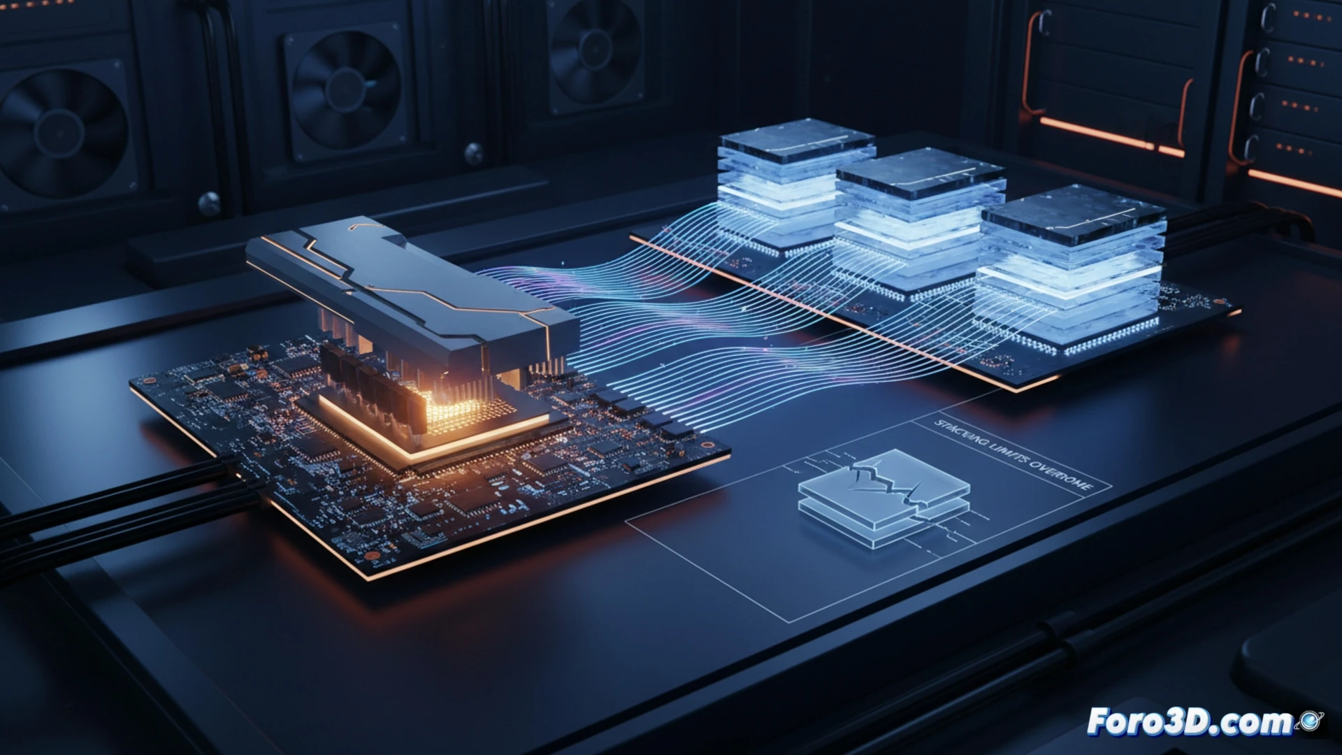
HBM memory manufacturers are planning a concept change: physically separating the memory chips from the GPU, placing them on an independent board. To avoid losing speed, they will use optical interfaces. The goal is to multiply the available capacity per GPU, surpassing the limit of stacking 16-20 layers or surrounding the memory chip, which makes the design more expensive.
Optical interfaces to break the physical bottleneck 🚀
Currently, HBM memory is stacked vertically and placed next to the GPU, which limits total capacity and complicates packaging. The new proposal decouples both components: the memory would go to a separate board, connected via high-speed optical links. This allows adding more modules without increasing silicon area or heat, and makes it easier to scale capacity for AI and HPC workloads.
Memory moves to another board: goodbye to overcrowding 😅
So HBM memory, tired of living stuck to the GPU like a barnacle, has decided to move to its own place. With fiber optics in between, the GPU will no longer have to put up with its noisy neighbors. Engineers, excited, calculate they will be able to stack modules until the budget screams enough. Of course, the wiring promises to be as fun as assembling a fiber optic Christmas tree.