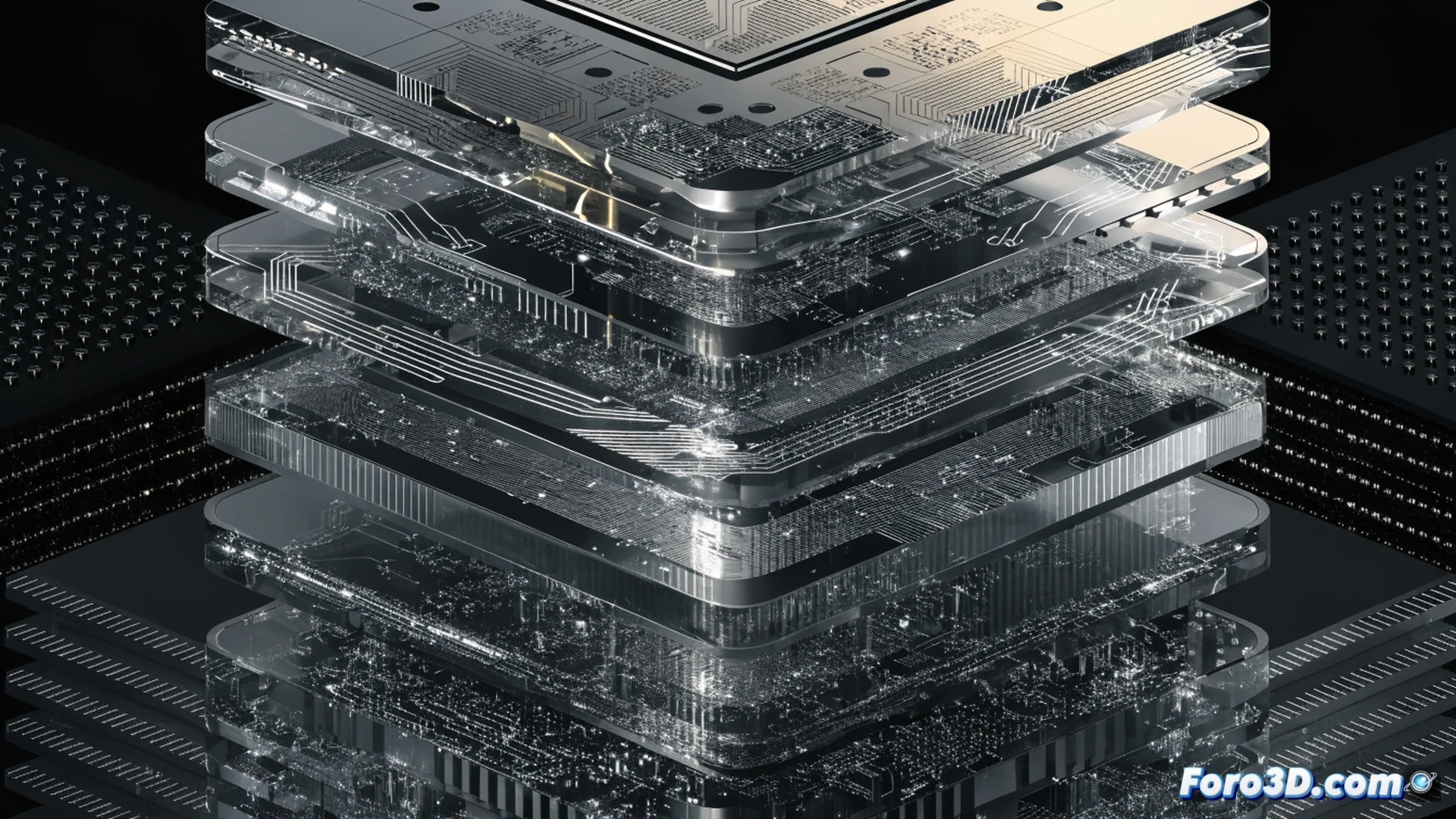
IBM has unveiled a fingernail-sized chip prototype that integrates nearly 100 billion transistors. The key lies in a 3D stacking technique that places two layers of silicon on top of each other. This design promises 70% more energy efficiency and 50% more performance than current chips, although its arrival in commercial devices is estimated to be about ten years away.
Two layers of silicon to double performance 🚀
The breakthrough is based on the vertical integration of transistors using the VTFET (Vertical Transport Field Effect Transistor) technique. By stacking two layers of silicon, electrons travel vertically, reducing travel distance and energy consumption. This allows more transistors to be packed without increasing the chip area, achieving a density that current planar methods cannot reach. The process requires advanced lithography and new materials, which explains the long development timeline.
Your phone in ten years: same size, more battery life 🔋
So, in a decade, your phone could have a battery that lasts a day and a half instead of one. Quite an advancement. Meanwhile, IBM engineers will keep stacking silicon like Lego towers, and we'll keep charging our phones at six in the evening. But hey, at least the future promises you won't have to look for an outlet so often.