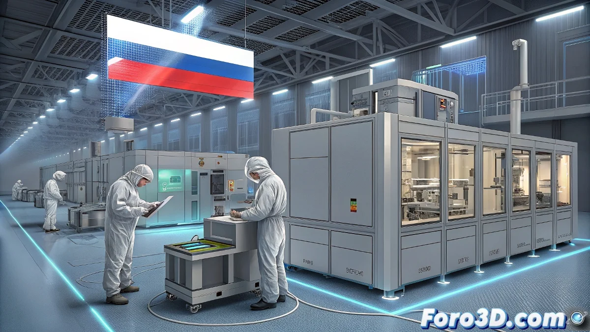
Russia Enters the Extreme Lithography Race
In a strategic move to achieve technological autonomy, Russia has presented an ambitious plan to develop its own extreme ultraviolet (EUV) lithography technology, key to manufacturing advanced chips. This project, extending until 2037, proposes a radically different architecture from that of ASML, the current monopolist in the sector, using alternative approaches in light generation and optical design. It is a bold attempt to break a critical dependency. 🇷🇺
A 15-Year Technology Roadmap
The plan is structured in three clearly defined phases, seeking incremental but steady development of capabilities:
- Phase 1 (2026-2028): Development of a system capable of 40 nm processes, laying the technological foundations.
- Phase 2 (2029-2032): 28 nm scanner (with potential for 14 nm), significantly increasing precision and performance.
- Phase 3 (2033-2036): System for nodes below 10 nm, with a complex six-mirror optical architecture.
Each stage has very specific precision and productivity objectives. 📅
Key Technical Differences with ASML
The Russian proposal is not a copy, but an alternative approach that seeks to avoid some of the complexities of ASML's technology. The main differences are fundamental:
- Light Source: Instead of using tin droplets to generate plasma, it uses xenon plasma, which theoretically reduces debris contamination.
- Wavelength: Operates at 11.2 nm, compared to ASML's standard 13.5 nm, requiring completely new optics.
- Simplification: Avoids the need for immersion lithography and multi-patterning techniques in advanced nodes.
It is a design that prioritizes robustness over compatibility with the global standard. ⚙️
The Russian approach uses xenon plasma, which eliminates debris that damages photo-masks and significantly reduces maintenance.
The Huge Challenges Ahead
Although the plan seems more realistic than previous attempts, the path is full of obstacles. The biggest challenge is the choice of a non-standard wavelength (11.2 nm), which forces the development of an entire supply chain from scratch: special ruthenium and beryllium mirrors, specific light sources, and compatible photoresists. Additionally, it remains to be seen whether the project, even if technically successful, will be able to compete commercially or if it will be destined solely for the Russian domestic market. 🤔
In the end, this announcement demonstrates that the geopolitics of semiconductors is becoming multipolar. And who knows, maybe by 2037 the question will not be who has the best EUV technology, but how many different standards will coexist in the market. 😉