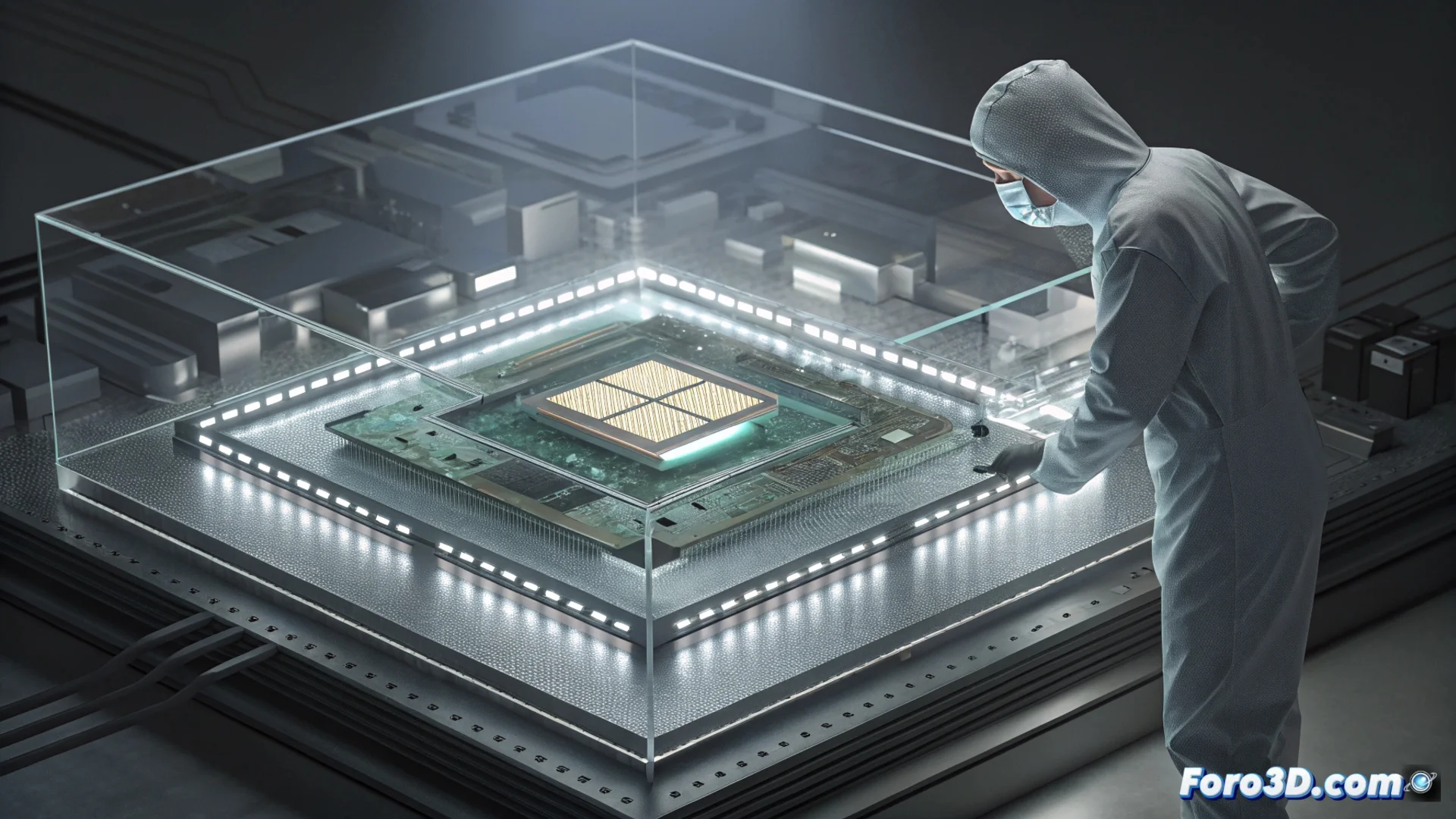
Imec Integrates HBM Memory Directly onto a GPU Substrate
At the IEDM event, the research center Imec unveiled an advance that could redefine how computing accelerators are built. Its prototype demonstrates fabricating HBM memory directly on the silicon substrate of a graphics processing unit. This method, called HBM on GPU, aims to eliminate the intermediate silicon component that currently connects the GPU to stacked memory modules. The result is a shorter path for signals, boosting performance and optimizing energy use, two pillars for artificial intelligence and high-performance computing. 🚀
The Technological Base: TSMC's 3D SoIC
This development doesn't start from scratch. It relies on TSMC's 3D SoIC integration technology. To test it, Imec created a test chip that joins a logic die fabricated on the 3nm N3 node with four stacked DRAM dies. The magic happens in the connection: they use copper microbumps with a minimum height of just 6 micrometers. This hybrid bonding process achieves enormous interconnection density, exceeding 10,000 connections per square millimeter. The final structure is more compact and positions itself as more efficient than conventional HBM solutions that rely on a passive interposer.
Key Features of the Prototype:- Architecture: One logic die (GPU) on N3 node connected to four stacked DRAM memory dies.
- Connection Technology: 6µm copper microbumps enabling high-density hybrid bonding.
- Main Advantage: Eliminates the silicon interposer, simplifying the design and shortening electrical paths.
Integrating memory directly onto the graphics processor substrate simplifies the system design and reduces packaging complexity.
Benefits and Challenges of Direct Bonding
Joining memory and logic on the same substrate brings tangible advantages. Simplifying the system design and reducing packaging complexity are the first ones. By drastically shortening interconnection paths, signals attenuate less and require less