Intel Foundry Details Its Specialized Hardware for AI and HPC
Intel's manufacturing division has released a technical report explaining how it designs and produces physical components dedicated to executing artificial intelligence and high-performance computing tasks. The document is accompanied by the presentation of a validation chip that demonstrates its current ability to integrate multiple elements into a single device. 🧠
Advanced Manufacturing and Packaging Options
The disclosed material specifies the production alternatives that Intel Foundry offers to its clients. This includes data on cutting-edge manufacturing nodes, such as Intel 18A, and methods for combining multiple chiplets or silicon fragments. The goal of these solutions is to build more powerful and efficient systems by uniting computing cores, fast memory, and interconnect elements into a single package.
Key Details from the Document:- Description of the most advanced process nodes available.
- Technologies for efficiently integrating multiple chiplets.
- Focus on creating complete and optimized systems in a single package.
The test chip is a crucial first step to validate technologies before large-scale production.
Validation of 3D Packaging Capabilities
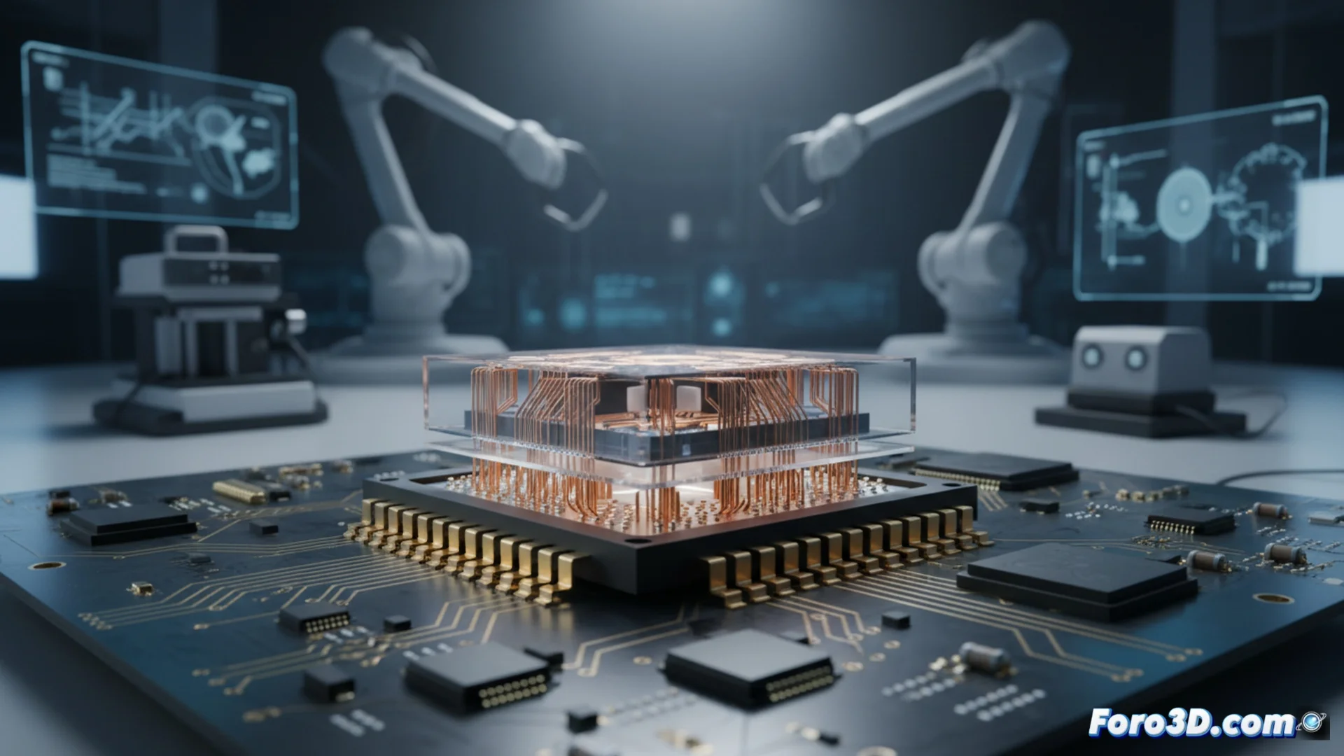
The AI prototype that Intel showcases incorporates several fundamental innovations. It uses the PowerVia architecture to manage power distribution and Foveros Direct technology to bond chips in 3D using copper connections. This strategy allows stacking components, such as processors and memory modules, to shorten the distance data travels and thus optimize both performance and energy consumption.
Technologies Implemented in the Test Chip:- PowerVia architecture for more efficient power delivery.
- Foveros Direct for high-density 3D copper interconnects.
- Ability to stack components and reduce latencies.
A Step Toward Commercial Future
Although the technical report is extensive and detailed, the validation chip represents only the initial phase of this journey. There is still a long way to go before these advances materialize into final products that reach the market and users can purchase. The document underscores Intel's commitment to pushing the boundaries of specialized hardware for the most demanding computational needs. ⚙️