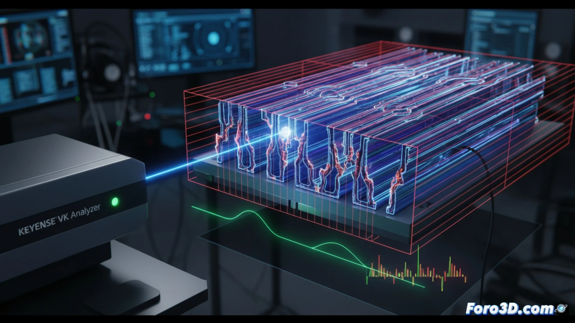
Quantum coherence is the soul of next-generation radar, but a micro-machining defect in the waveguide can destroy it. Researchers have used 3D profilometry with the Keyence VK Analyzer to identify sub-micrometric roughness on the internal wall of the component. These imperfections, invisible to conventional optical inspection, generate scattering and phase loss in entangled photons, degrading the quantum radar signal. The finding demonstrates how precision metrology becomes an indispensable tool for quantum hardware validation.
Modeling and simulation of electromagnetic impact in COMSOL 🧠
To quantify the damage, the team digitized the defect profile using the Keyence VK Analyzer and exported the point cloud to SolidWorks, reconstructing a waveguide with the actual imperfection. Subsequently, the geometry was imported into COMSOL Multiphysics to simulate the propagation of the fundamental TE10 mode. The results showed an 18% drop in transmitted power and a phase shift of 0.7 radians in the carrier signal, critical values that break quantum entanglement. The simulation confirmed that the surface roughness tolerance must be less than 50 nanometers to maintain coherence, a standard that demands rethinking machining processes in the semiconductor industry.
Lessons for microfabrication of quantum components 🔬
This case highlights an uncomfortable reality: the boundary between chip manufacturing and quantum optics is blurring. A simple milling error in a waveguide can invalidate an entire radar system. The solution lies not only in better machines but in integrating 3D profilometry as an online quality control. If the semiconductor industry wants to scale quantum devices, it must adopt machining tolerances inherited from extreme lithography, where every nanometer counts. The future of quantum radar hinges on the precision of surface roughness.
As a cleanroom process engineer, what surface roughness threshold measured by 3D profilometry do you consider critical to guarantee quantum coherence in gallium arsenide waveguides at terahertz frequencies?
(PS: at Foro3D our favorite lithography is printing filament layers)