In the summer of 2023, NASA's Deep Space Network suffered a critical transmitter failure during a mission to Jupiter. The symptom was an intermittent loss of power in the gold waveguide. After a thorough 3D analysis with CST Studio Suite, engineers discovered the cause: a microscopic dust particle, trapped during cleanroom assembly, that triggered the multipactor phenomenon. This defect, invisible to the human eye, generated micro-sparks that degraded the signal.
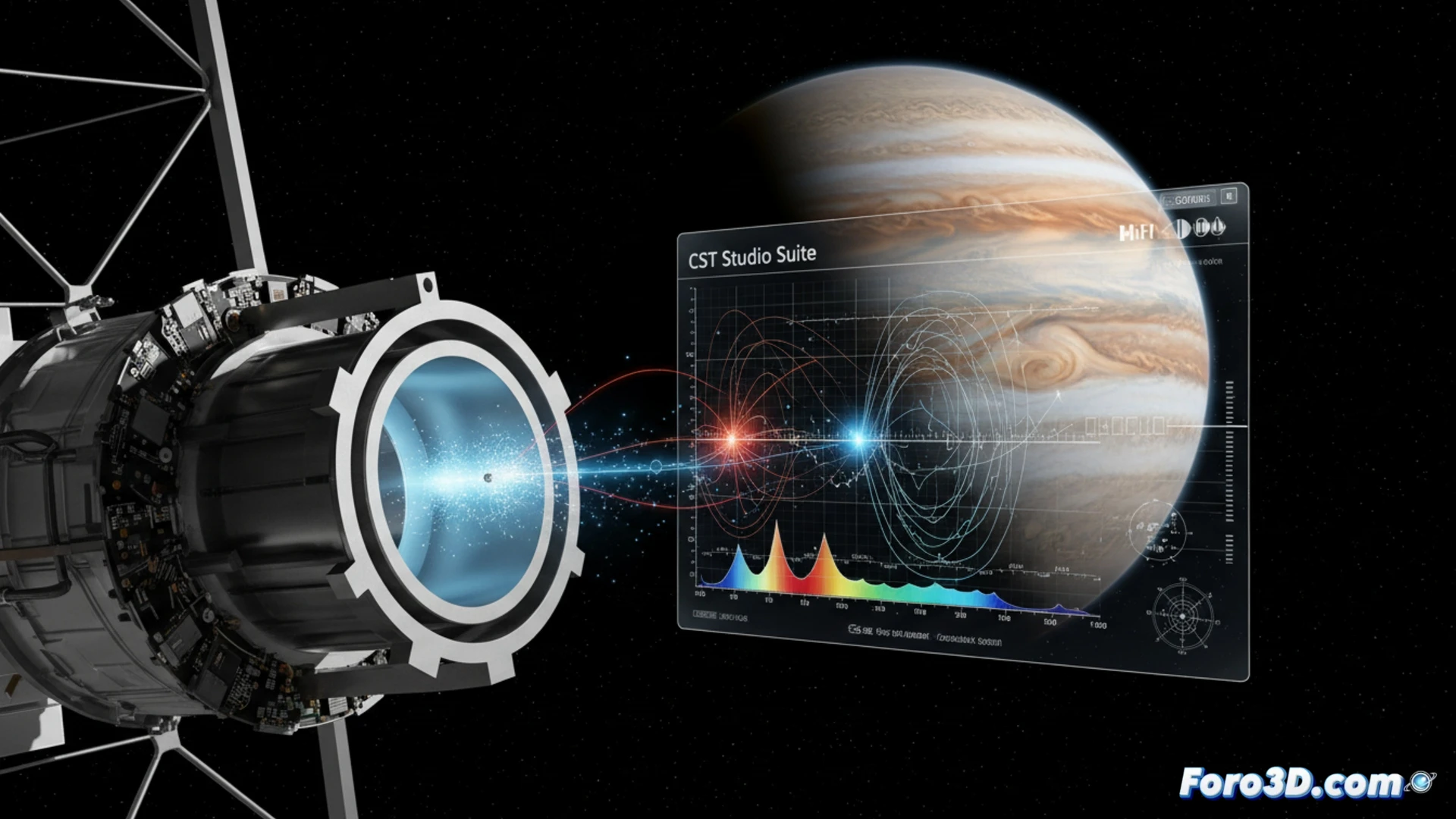
Multipactor and electromagnetic simulation in gold waveguides 🛰️
Multipactor is a resonant electron discharge that occurs under vacuum and high RF power conditions. In this gold-plated waveguide, the dust particle acted as a secondary electron emission point. Using CST Studio Suite, the team modeled the electromagnetic field in 3D and reproduced the electron trajectory within the duct. The simulation revealed an exact resonance between the signal frequency and the electron flight time, amplifying the effect until it caused a localized electrical arc. Subsequent visualization in KeyShot allowed mapping of the highest current density zones and erosion marks on the gold.
Microfabrication lessons for aerospace reliability 🔬
This case demonstrates that particle contamination in cleanrooms remains the Achilles' heel of high-reliability components. Although gold is chemically inert, its surface does not tolerate geometric defects at the micrometer scale. The 3D analysis not only identified the failure but also validated the need for stricter inspection protocols in waveguide microfabrication. For the semiconductor and aerospace components industry, tools like Materialise Magics are essential for detecting these anomalies before final assembly.
Can 3D microfabrication of dielectric shields at the micrometer scale prevent the formation of dust-induced electrical arcs in high-power transmitters for deep space?
(PS: modeling a chip in 3D is easy; the hard part is making it not look like a Lego city)