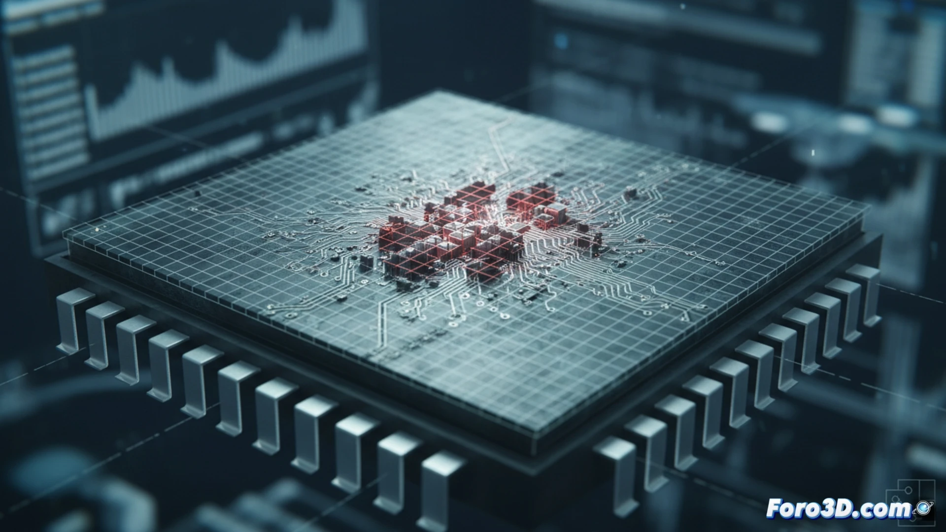
Security in the semiconductor supply chain faces a growing threat: hardware trojans. These malicious modifications, invisible to the naked eye, alter the chip's functionality. The combination of high-resolution 3D microscopy, such as that offered by ZEISS ZEN, and image analysis with MATLAB, allows inspecting the micro-topography of a sabotaged chip to identify nanometric anomalies that reveal its presence.
Workflow: From nanometric imaging to design verification 🔬
The process begins with capturing the chip's surface topography using scanning electron microscopy, generating a 3D map of the structure. Using ZEISS ZEN, the circuit morphology is reconstructed with subnanometric precision. Then, MATLAB processes these images by applying edge detection filters and correlation algorithms to locate deviations in layer thickness or via geometry. Finally, the detected anomalies are compared with the original design verified in Synopsys. Any undocumented structure, such as an extra logic cell or a displaced metal path, is identified as a possible trojan, validating the chip's integrity against physical attacks.
Inspection as a barrier against silent sabotage 🛡️
The ability to analyze micro-topography at the atomic level redefines security in 3D microfabrication. This forensic approach not only detects trojans but also allows auditing the supply chain, from the foundry to assembly. For semiconductor engineers, mastering these visualization and verification tools is essential. The question is no longer whether a chip can be sabotaged, but whether we have the technology to discover it before it causes a catastrophic failure.
How can 3D micro-topography distinguish between a natural variation in the lithographic process and the intentional alteration of a hardware trojan in state-of-the-art chips?
(PS: 180nm are like relics: the smaller they are, the harder to see with the naked eye)