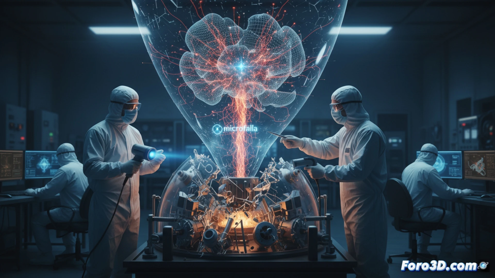
A carbon vapor explosion has destroyed a nanotechnology laboratory, but the real challenge is not the cleanup, but locating the exact point of failure in the chemical vapor deposition (CVD) chamber. The forensic team has deployed a 3D pipeline combining industrial computed tomography, scene scanning, and computational fluid dynamics to reconstruct the trajectory of fragments at a microscopic scale and determine the root cause of the accident.
Reconstruction pipeline: from CT to CFD simulation 🔬
The process begins with scene scanning using FARO Scene, capturing the spatial distribution of debris. In parallel, reactor fragments are analyzed with Volume Graphics VGSTUDIO MAX, industrial CT software that allows inspection of porosity and microcracks in the chamber walls. With this data, the geometry is imported into Autodesk CFD to simulate gas flow at the instant before the explosion. The simulation reveals points of carbon vapor pressure buildup. Finally, Rhino 3D traces the ballistic trajectories of the fragments, correlating their ejection vector with the origin point identified in the CFD. The result is a forensic map pointing to a faulty weld in the chamber seal as the catastrophic failure point.
Digital twin and prevention in semiconductor microfabrication ⚙️
This accident underscores the need to integrate digital twins into chemical vapor deposition processes. Beyond forensic reconstruction, using tools like VGSTUDIO MAX and CFD allows simulating extreme conditions before operating the actual reactor. In the semiconductor industry, where a single particle can ruin a batch of wafers, predicting structural failures or blockages in the flow of gaseous precursors is critical. Adopting this 3D pipeline not only clarifies incidents but establishes a data-driven safety protocol for cleanrooms and CVD reactors.
Can the 3D reconstruction of the trajectory of silicon wafer fragments and the distribution of graphitic particles reveal whether the explosion was caused by a pre-existing microcrack in the CVD reactor or by a sudden overpressure during graphene growth?
(PS: simulating a 200mm wafer is like making a pizza: everyone wants a slice)