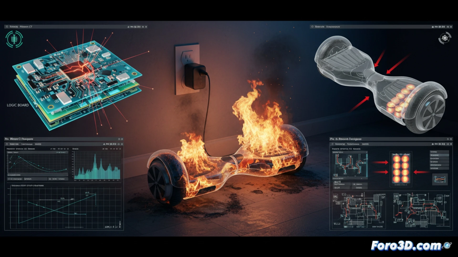
A self-balancing scooter caught fire during routine charging. Forensic analysis using 3D X-ray with a Nikon CT system and Dragonfly software revealed the root cause: a short circuit between internal layers of the PCB. The copper traces, designed with insufficient spacing, generated an electrical arc that led to localized overheating, triggering the thermal disaster.
Defective microfabrication: the problem of traces too close together 🔥
The volumetric reconstruction of the PCB in Dragonfly allowed visualization of the exact failure point. By importing the model into Altium Designer, it was confirmed that the original design violated the minimum spacing rules between conductors for the operating voltage. This DFM (Design for Manufacturing) error created a high current density zone. The 3D thermal simulation showed that, without adequate dielectric barriers between layers, the heat generated by the short concentrated in a critical area. The 3D model of the chassis, rendered in Blender, demonstrated the absence of thermal barriers between the board and the lithium cells. This design allowed the short's temperature to propagate heat directly to the battery pack, initiating the chain reaction of the fire.
Lessons for semiconductor and PCB design ⚡
This incident underscores the importance of spacing rules and signal integrity analysis in the microfabrication of control boards. The separation between traces is not just an electrical parameter; it is a thermal safety barrier. Tools like Altium Designer allow simulating these scenarios before production, detecting risk zones. Ignoring DFM rules to reduce costs or PCB size not only compromises semiconductor functionality but, as in this case, can turn an everyday device into an ignition source.
Is it possible to detect interlayer shorts in multilayer PCBs using 3D X-ray without destructive cross-sectioning, and if so, what scanning parameters are critical to differentiate a short from a copper thickness variation in forensic failure analysis of high-density devices like hoverboards?
(PS: 180nm are like relics: the smaller they are, the harder to see with the naked eye)