Apple's Private Cloud Compute (PCC) architecture marks a milestone at the intersection of artificial intelligence and hardware security. This system is not a simple data center; it is a custom silicon infrastructure where each server, based on Apple Silicon, functions as an isolated fortress. The key lies in the Secure Enclave, a coprocessor that manages data encryption at rest and in transit, ensuring that not even Apple can access user information during the processing of AI requests.
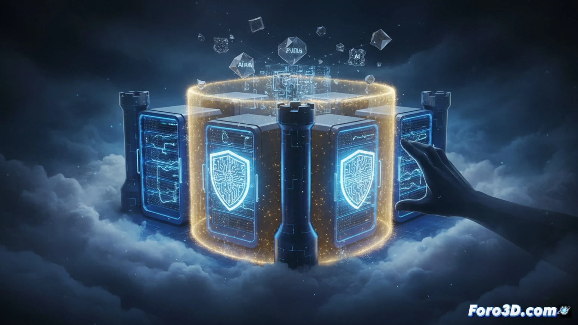
Silicon architecture: Isolation and cryptographic verification 🔒
Each PCC server is built on an M2 Ultra chip array, integrating multiple CPU, GPU, and Neural Engine cores. The innovation lies in the physical and logical separation of data: when a request enters the system, the Secure Enclave generates an ephemeral session key. Processing occurs within a Trusted Execution Environment (TEE) that isolates RAM and SSD storage from the rest of the system. To ensure transparency, Apple implements a remote attestation mechanism; any external operator can cryptographically verify that the software on the chip is exactly the code signed by Apple, without malicious modifications. This data flow can be modeled in 3D as a cascade of transistors where light (data) only illuminates a strictly defined path before self-destructing.
The manufacturer's dilemma: Raw power versus radical privacy ⚖️
Apple's decision to use proprietary silicon instead of mass-market GPUs (such as those from NVIDIA) reveals a design strategy focused on control. While M2 Ultra chips offer lower AI performance compared to H100 clusters, their unified architecture enables memory isolation that is impossible to replicate in standard x86 systems. For the semiconductor industry, this raises a fundamental question: are we willing to sacrifice computing speed for total integrity verification? Apple's answer is a server that, instead of maximizing teraflops, optimizes the hermetic sealing of each piece of data, transforming cloud computing into a vacuum-sealed device.
Since Apple's Private Cloud Compute architecture relies on the security of the Secure Enclave, what innovations in 3D microfabrication would allow integrating such trust modules directly into the silicon substrate of server chips, improving resistance against physical and side-channel attacks?
(PS: integrated circuits are like exams: the more you look at them, the more lines you see)