Elon Musk announced Terafab, an ambitious chip manufacturing plant in Austin for Tesla and SpaceX. Its goal is to produce semiconductors on a massive scale for AI, robotics, and space data centers. However, the project faces an immense reality: building a foundry requires tens of billions, years of development, and a expertise that Musk lacks. The absence of a concrete timeline adds more unknowns to this technically colossal plan.
The Critical Role of 3D Modeling in Foundry Design 🏗️
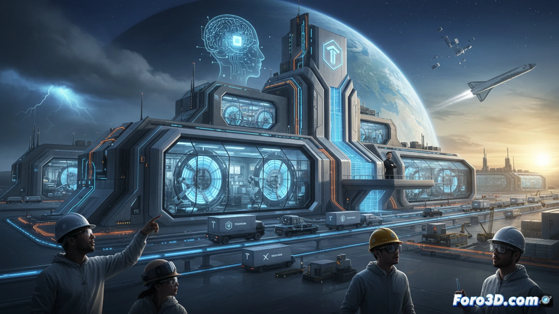
Designing a semiconductor factory like Terafab is unthinkable without advanced 3D modeling and simulation tools. These are crucial for planning the cleanroom layout, an environment of extreme purity where the slightest airflow error or vibration ruins entire batches. 3D simulation of processes like extreme ultraviolet (EUV) lithography allows optimizing performance before installing equipment that costs hundreds of millions. Additionally, visualizing the internal architecture of chips, with their nanometric 3D interconnections, is fundamental for design and production planning.
Ambition vs. Reality in Microfabrication ⚖️
The gap between Musk's vision and technical execution is abysmal. While he talks about exaflops of space computing, the semiconductor industry struggles with quantum physics, materials, and production yields. Terafab is not a car or a rocket; it is an ultra-high-precision ecosystem where mastering chemical and physical processes takes decades. Without an established technological partner and without prior experience, the project seems more like a statement of intent than an executable plan, underscoring that in microfabrication, 3D modeling is the guide, but process mastery is the law.
How could Terafab's extreme vertical integration, from design to 3D packaging, redefine performance and cost parameters for automotive and aerospace chips?
(P.S.: simulating a 200mm wafer is like making a pizza: everyone wants a slice)