The suspension of operations at Tower Semiconductor in Israel has triggered a contingency plan in the semiconductor supply chain. As a foundry specialized in mature nodes, its halt forces automotive and industrial customers to urgently relocate their orders. The similar capacity of the Taiwanese PSMC in 200 mm wafers and processes from 180 to 130 nm makes it the natural destination, saturating its lithography lines and generating immediate upward pressure on contract manufacturing prices in this segment.
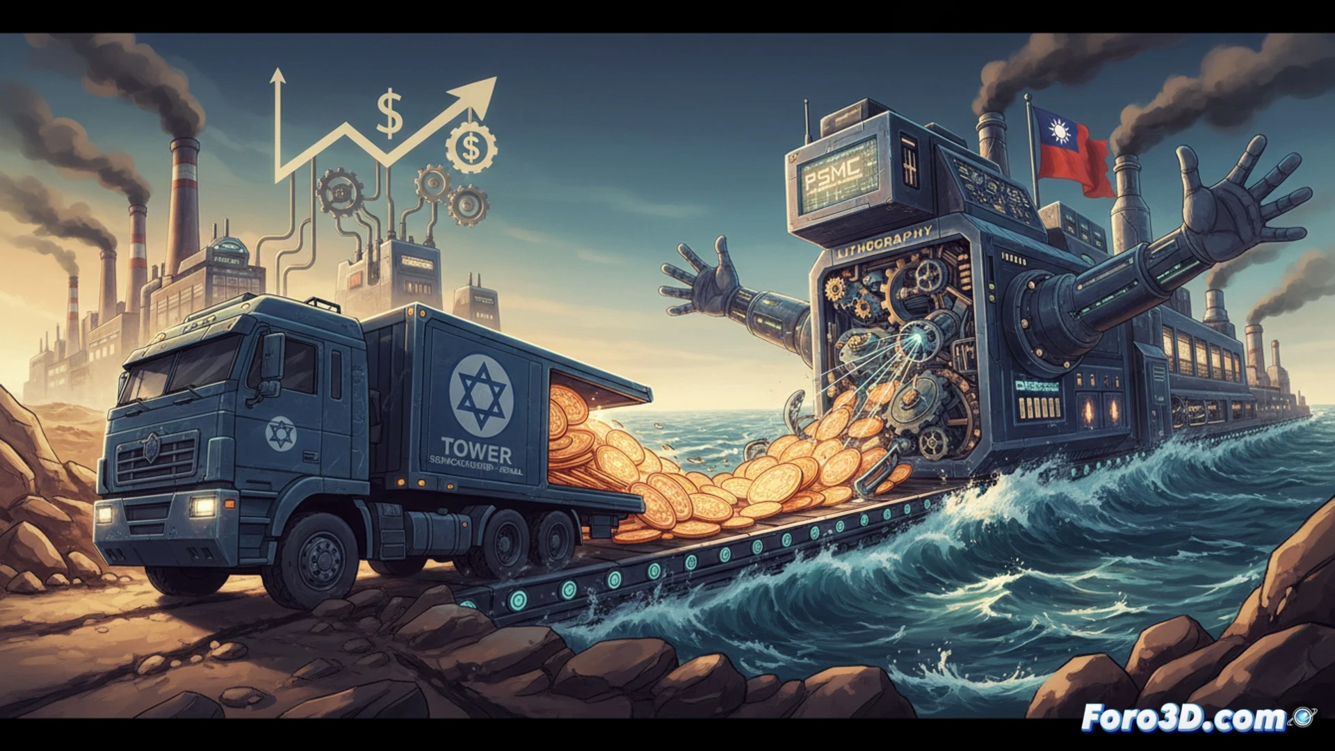
Visualizing the transfer: 200 mm wafers and mature nodes (180-130 nm) 🔍
To model this scenario, we must visualize the affected production line. Tower's plant operates with 200 mm diameter silicon wafers, where successive layers are printed via photolithography to create chips with features measured in nanometers. Its specialty is mature processes, between 180 and 130 nm, crucial for microcontrollers, sensors, and power chips. When this line stops, a virtual flow of in-process wafers is diverted to equivalent facilities, such as those of PSMC or Vanguard. The 3D simulation would show how lithography machines, masks, and diffusion furnaces in Taiwanese foundries increase their utilization rate, creating bottlenecks in specific process stages, which justifies the cost increase.
The resilience of the chain depends on mature capacity ⚙️
This event underscores the critical dependence of industries like automotive on established manufacturing technologies. The disruption in a geopolitically unstable node proves that redundancy in mature lithography capacity is a strategic asset. Taiwan's rapid absorption of demand mitigates shortages but reveals a fragile network. Visualizing the wafer flow is not just a technical exercise, but a tool for planning resilience in a sector where the old remains indispensable.
How does the reallocation of wafer production from Israel to Taiwan affect the capacity and costs of mature node lithography globally?
(P.S.: at Foro3D our favorite lithography is filament layer printing)