The IEEE Institute, along with universities such as UCLA and USC, has launched microcredential programs in semiconductors. These courses, which include practical training in clean rooms, aim to urgently cover the talent gap in the industry. In this context, 3D visualization and simulation emerge as fundamental pedagogical tools. They allow students to interact with detailed models of wafers, equipment, and manufacturing processes before stepping into expensive facilities, accelerating understanding and reducing risks.
3D Modeling of Processes: The Essential Educational Simulator 🔬
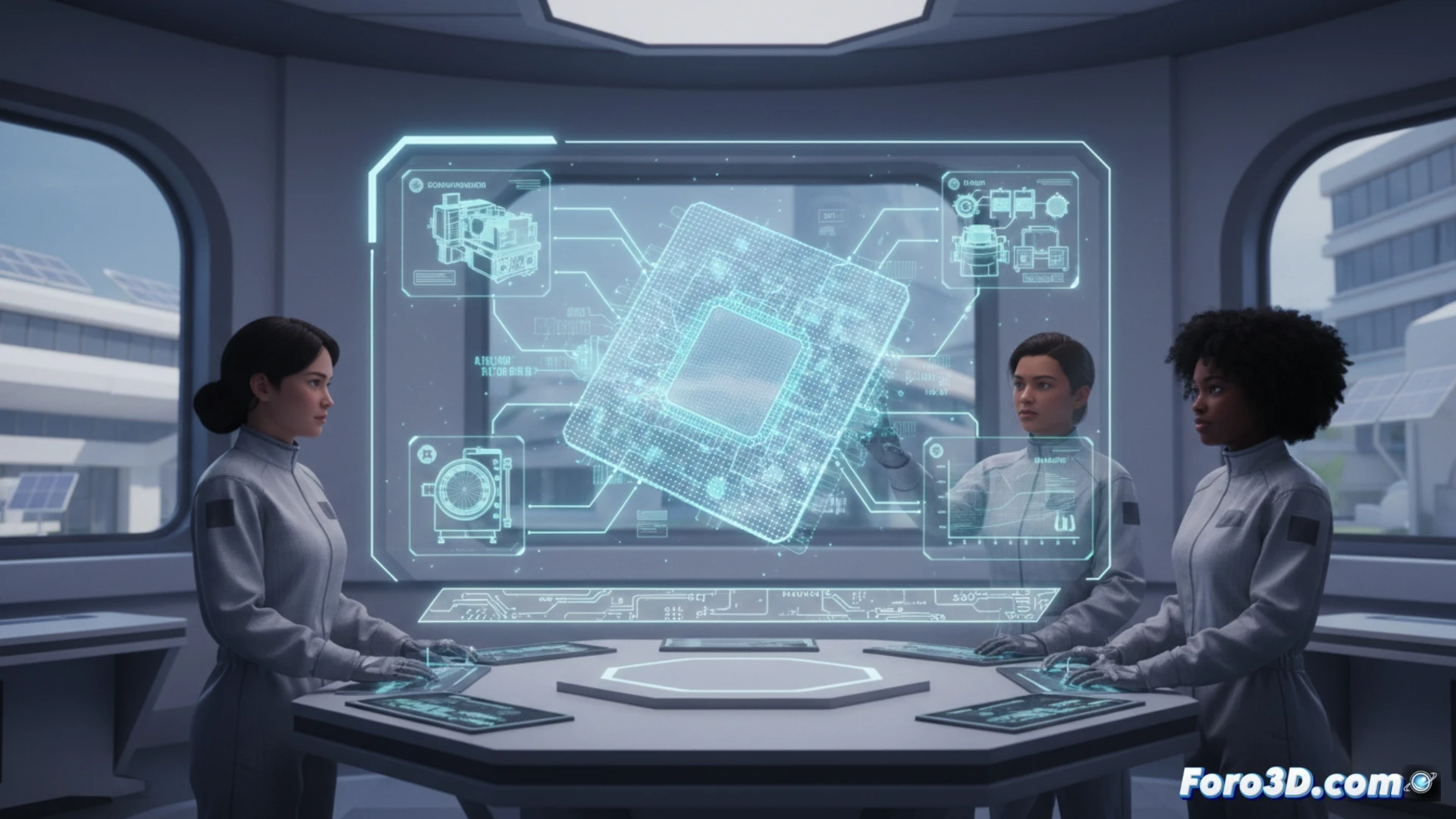
Microfabrication involves complex processes and critical sequences, such as layer deposition, lithography, or etching. Here, 3D modeling is an indispensable cognitive bridge. Through interactive simulations, students can visualize the internal architecture of a chip, the material flow in a vacuum chamber, or the precise alignment of a mask. This virtual learning layer not only demonstrates how it is done, but why each step is crucial. It facilitates the assimilation of abstract and costly concepts, optimizing valuable time in the real clean room and preparing technicians with deep and spatial knowledge of the processes.
Beyond the Clean Room: A New Training Standard 🚀
The integration of these 3D tools into curricula establishes a new paradigm in technical training. It is not just about learning to operate equipment, but about holistically understanding the manufacturing ecosystem. This methodology, driven by IEEE, not only quickly trains new talents but also elevates the level of specialization. By closing the gap between theory and expensive practice, 3D visualization consolidates itself as the pillar to build the expert workforce that the semiconductor industry demands.
How are interactive 3D visualization tools transforming training in semiconductor design and manufacturing to close the talent gap in the industry?
(P.S.: at Foro3D our favorite lithography is filament layer printing)