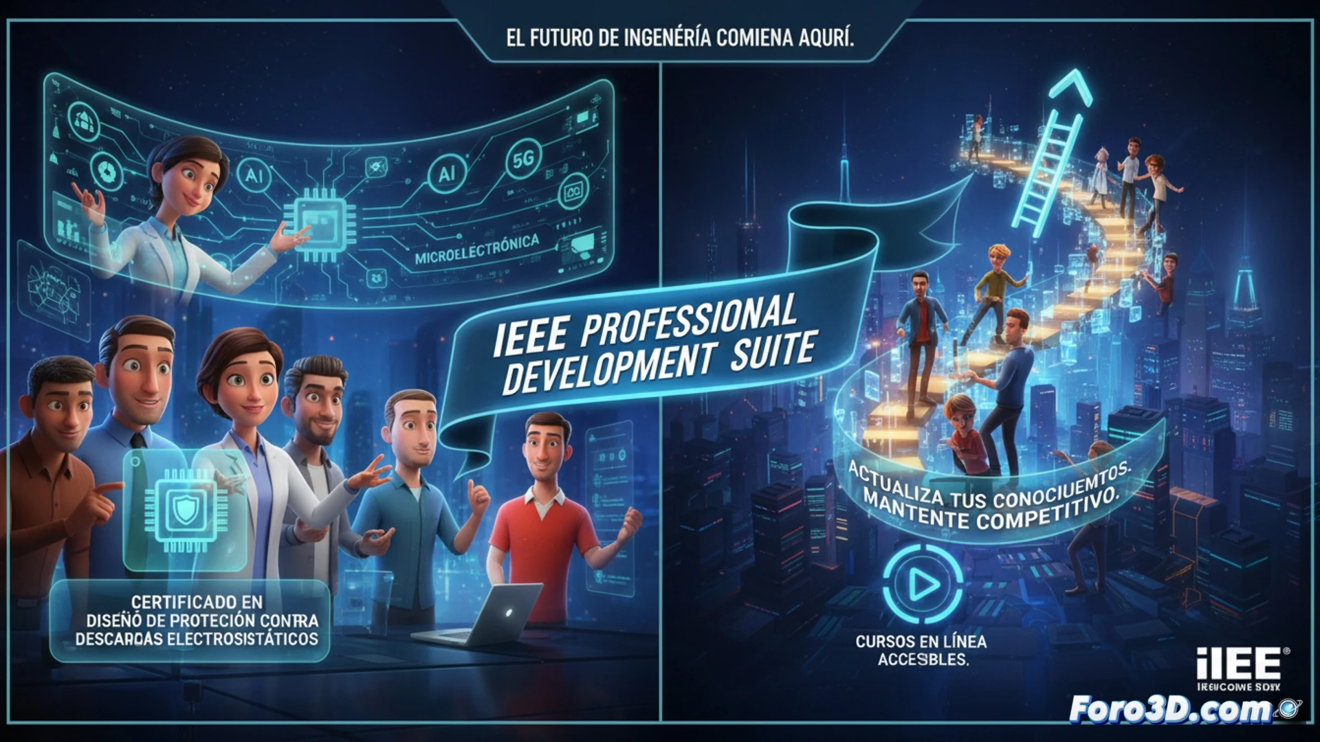
The IEEE has launched a professional development suite with specialized courses for the semiconductor sector, including a certificate in electrostatic discharge protection design. In a field where architectural complexity is extreme, effective training goes beyond manuals. This is where 3D visualization and simulation tools become indispensable, allowing engineers and technicians to internalize abstract concepts through interactive models of wafers, transistors, and signal paths, aligning with the need for practical and in-depth learning.
From Theory to Wafer: 3D Simulation for ESD and Process Planning 🧠
Programs like the ESD protection certificate cannot be taught solely with equations and flat diagrams. The physical layout of protection devices, their paths in the multiple layers of a chip, and their interaction with the substrate require spatial understanding. 3D modeling tools allow visualizing the complete integrated circuit architecture, simulating electrostatic charge flow, and virtually planning wafer fabrication. This reduces costly errors and facilitates the design of more robust structures. 3D simulation thus becomes the essential bridge between the theoretical knowledge imparted in courses and its real application in the cleanroom.
Continuous Training Demands Mastering the Spatial Dimension 🚀
Staying competitive in microelectronics no longer depends solely on knowing the latest materials or fabrication nodes. It involves mastering the technologies that enable understanding that fabrication. Continuous professional development, as promoted by the IEEE, must inevitably integrate training in 3D visualization software. Those who cannot interpret or create three-dimensional models of processes and circuits will be at a disadvantage, as this is the modern lingua franca for designing, collaborating, and optimizing in the era of 3D integration and heterogeneous chips.
How can interactive 3D visualization transform training in semiconductor design and manufacturing to overcome the limits of 2D abstraction?
(P.S.: 180nm are like relics: the smaller they are, the harder they are to see with the naked eye) 👓