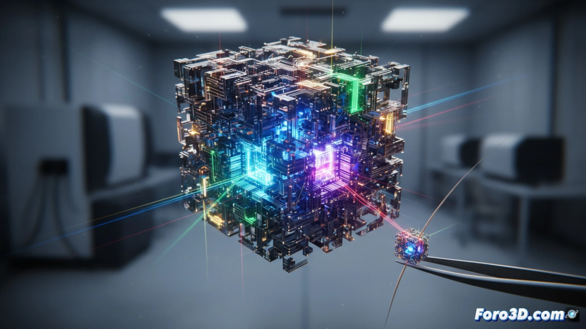
Researchers at the University of Sydney have created a prototype of a nanoscale photonic artificial intelligence chip. This device, as thick as a human hair, replaces electrons with photons to perform calculations, promising a revolution in energy efficiency. The key to its operation lies in the neural network being physically encoded in the chip's nanostructures, which are designed and modeled in 3D to guide light and execute mathematical operations at picosecond speeds.
3D Architecture and Fabrication of the Light-Guiding Nanostructures 🔬
The innovation is not only in materials, but in microscale architecture. The neural network materializes as a maze of waveguides, splitters, and photonic resonators etched into the chip. Designing this optical circuit requires advanced 3D modeling to accurately simulate how photons propagate and interfere in structures smaller than the wavelength of light. Fabricated at the Sydney Nano Hub, the process involves high-precision lithography and 3D etching techniques to sculpt these nanostructures into the substrate, physically defining the computing function. Light, as it passes through this frozen circuit, executes the network's operation without the need to run sequential software.
The Critical Role of Simulation and 3D Modeling 💡
This advance underscores the critical importance of 3D design and simulation at the forefront of microfabrication. Before any physical etching, researchers must virtually model and validate the behavior of light in such complex architectures. Electromagnetic simulation and 3D modeling tools are, therefore, the digital workshop where these processors are conceived. Without this ability to preview and optimize the nanoarchitecture in three dimensions, materializing a physical concept of optical computing would be impossible, marking a path where 3D design and fabrication are a single discipline.
How does 3D nanofabrication overcome the limitations of traditional planar lithography to integrate photonic and electronic components in a nanoscale AI chip?
(P.S.: the 180nm are like relics: the smaller they are, the harder they are to see with the naked eye)