A fault in the magnet of a magnetic transport system not only stops levitation but also generates current spikes and stray fields that destroy power semiconductors. At Foro3D, we analyze how three-dimensional modeling of magnetic fields allows visualizing flux distortion and predicting fatigue in Hall sensors and MOSFETs, offering a precise map of the fault's origin before it occurs in the actual hardware.
3D simulation of magnetic fields and stress points in semiconductors 🧲
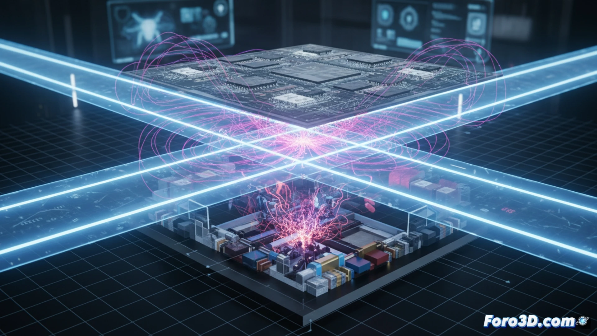
To model a magnet fault, a digital twin of the transport system is built in finite element software, such as COMSOL Multiphysics or Ansys Maxwell. The 3D geometry includes the permanent magnet or electromagnet, the reaction rail, and the control circuit with IGBTs and Hall sensors. By inducing a local demagnetization or a winding break, the model reveals how the residual magnetic field generates harmonics in the levitation coil. These harmonics raise the blocking voltage in the power transistors, exceeding their thermal limits. The simulation also shows that the magnetic flux density concentrates in asymmetric zones, causing saturations in the Hall sensors that send erroneous signals to the microcontroller, destabilizing the control loop.
Reflection on preventive design in 3D microfabrication ⚡
This 3D modeling approach allows semiconductor engineers to redesign the sensor layout and power circuit topology to tolerate partial magnet faults. By integrating electromagnetic simulation with control architecture visualization, critical current paths and thermal dissipation points are identified. The lesson is clear: a magnetic fault is not just a mechanical problem, but a cascade of electrical events that is only fully understood when observed in three dimensions.
How would you model in 3D the evolution of current spikes induced by a magnetic fault in a levitation system for semiconductors, and what key parameters should be included to simulate its impact on microfabrication?
(PS: at Foro3D our favorite lithography is printing layers of filament)