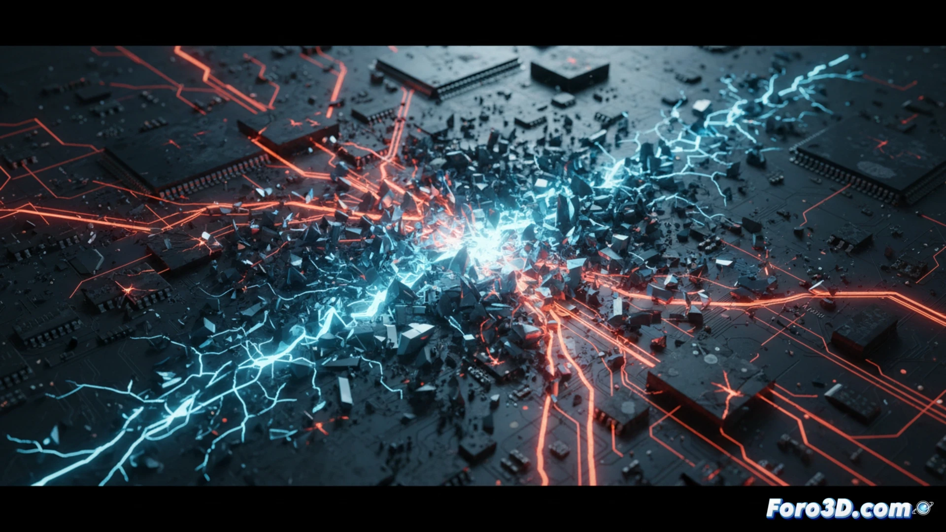
The fracture of a superconductor is not a simple mechanical tear; it is the visible manifestation of a catastrophe at the crystal lattice level. For a microfabrication specialist, this event represents a critical case study where thermal stresses and critical currents exceed the cohesive strength of the material. Here we analyze how the fracture is modeled in 3D and what lessons it offers for the design of high-performance chips.
Simulation of stresses in the crystal lattice and nucleation points 🧊
In the 3D modeling of a high-temperature superconductor (such as YBCO), finite element simulation reveals that the fracture usually initiates at grain boundaries. These points act as stress concentrators when the material experiences a quenching (sudden loss of superconductivity). Volumetric visualization allows identifying crack propagation along cleavage planes, a phenomenon analogous to cracking in silicon wafers during the dicing process. In quantum computing chips, where superconducting qubits operate at millikelvins, a microfracture of just a few microns can destabilize the entire Josephson circuit, leading to a critical error in quantum entanglement.
Lessons for 3D integration of quantum devices ⚛️
The fragility of these materials forces us to rethink encapsulation and anchoring strategies in cryogenic systems. Just as sacrificial layers are used in traditional semiconductors to relieve stresses, in superconductors the interfaces between the substrate and the thin film must be optimized. The fracture is not just a failure; it is visual feedback that teaches us to design more resilient structures, where 3D simulation prior to manufacturing becomes the standard to avoid collapses in the next generation of quantum processors.
As a microfabrication engineer, which parameters of 3D fracture modeling in superconductors are most critical for predicting catastrophic failures and avoiding crystal lattice rupture during the deposition process?
(PS: simulating a 200mm wafer is like making a pizza: everyone wants a slice) 🍕