Wafer-on-Wafer Bonding: The Extreme 3D Packaging Technique
In the pursuit of greater power and efficiency, the semiconductor industry is advancing toward the third dimension. One of the most radical methodologies is Wafer-on-Wafer (WoW) bonding, which fuses two complete silicon wafers before separating them into individual chips. This method contrasts with traditional approaches and enables unprecedented system integration. 🚀
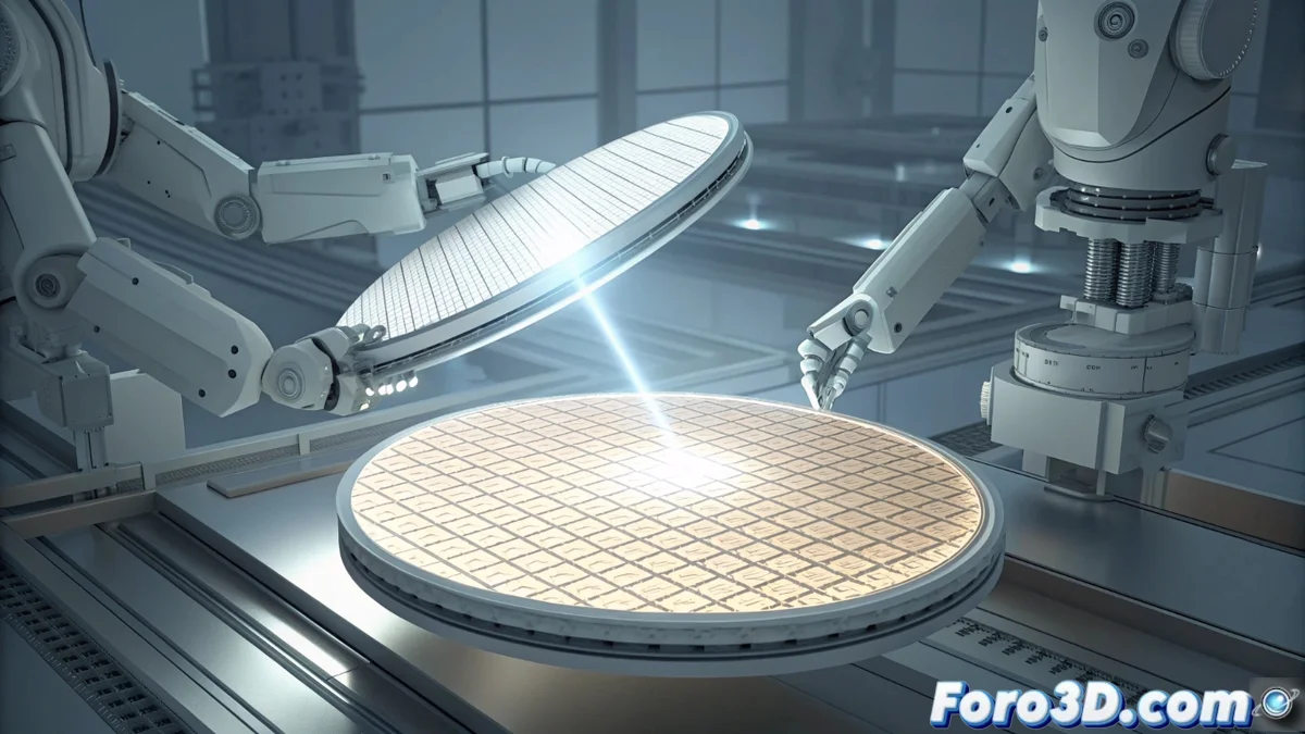
The Nanometric Bonding Process
The technique does not stack already diced chips, but operates at an earlier level. First, two wafers are processed independently, each with their own transistors and circuits. Then, a high-precision alignment system places them face-to-face with nanometric accuracy. Permanent bonding is achieved by applying controlled heat and pressure, creating a monolithic silicon block. Within this block, the electrical channels between the two halves are incredibly dense and short. Only after this fusion is the block diced to obtain the final 3D devices.
Key Advantages of WoW Bonding:- Extreme Interconnection Density: Wafer-level connection allows thousands of times more communication paths than with microbumps.
- Ultra-Short Signal Path: Data travels minimal distances between modules, accelerating transfer and reducing power consumption.
- Complete System Integration: Facilitates joining, for example, logic processing units and high-speed memory banks into a single compact device.
The real challenge is not bonding the wafers, but preventing them from sticking accidentally during manufacturing, a problem every engineer knows all too well.
Comparison with Other 3D Techniques
Methods like chip stacking (Chip-on-Chip) or the use of Through-Silicon Vias (TSVs) have inherent limitations. In those cases, vertical connections (microbumps or TSVs) are physically larger and more spaced apart, creating a bottleneck for communication. WoW bonding eliminates this obstacle by interconnecting the transistors of one wafer directly with those of the other at the microscopic scale. This transforms how information flows between the different functional blocks of a system.
Main Differences:- Connection Scale: WoW operates at the transistor/wafer level, while other techniques do so at the chip/packaging level.
- Vias Spacing: The interconnection density in WoW is orders of magnitude higher.
- Manufacturing Process: WoW bonds before dicing, which simplifies handling and alignment of extremely small components.
Challenges and Future of 3D Integration
Implementing this technology is not without obstacles. In addition to the risk of premature adhesion of the wafers, cleanrooms with exceptional cleanliness levels and very expensive alignment equipment are required. However, the reward justifies the effort: complete systems that are faster and more efficient, packaged in minimal space. This evolution is crucial to continue Moore's Law and power the next generation of computing, artificial intelligence, and mobile devices. WoW bonding represents a conceptual leap in how we build electronics. 💡