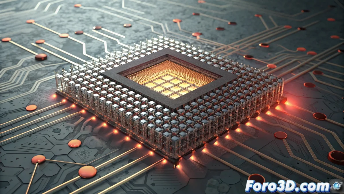
The revolution of gate-all-around (GAA) transistors: beyond FinFET
The evolution of semiconductors has entered a new critical phase with the arrival of the Gate-All-Around (GAA) architecture. This advance represents the direct and necessary successor to FinFET technology, which is reaching its limit in the most extreme manufacturing processes. The central idea is as elegant as it is powerful: while a FinFET controls the electric flow from three sides, a GAA transistor completely surrounds it, establishing a new paradigm of control at the atomic scale. 🚀
The power of absolute control: key advantages of GAA
The superiority of gate-all-around transistors lies in that total dominance over the conductive channel. This airtight enclosure allows for an infinitely more precise management of the current, which materializes in two monumental benefits. First, rest leakage currents are minimized, a headache that grows with every nanometer reduction. Second, unprecedented energy efficiency is achieved, allowing chips to operate at higher frequencies without turning into ovens or, alternatively, offering the same performance with a fraction of the consumption. 🔋
Main improvements over FinFET:- Improved electrostatic control: The gate surrounding the channel eliminates blind spots, improving switching.
- Drastic reduction in consumption: Lower operating voltage for the same performance, key for portable devices.
- Higher transistor density: Allows packing more logic in the same space, continuing the scaling.
GAA technology is not just one more step; it is the fundamental bridge to sustain Moore's Law in the next decade and power artificial intelligence and high-performance computing.
Industrial implementation and the path to angstroms
Semiconductor foundry giants like Samsung and TSMC have already begun mass production with 3 nanometer (3nm) nodes based on GAA, and their roadmap points to its refinement in future 2nm and even 1.4nm processes. The physical realization of this architecture can vary, using nanosheets stacked horizontally or nanowires, but the principle of the surrounding gate remains unchanged as the backbone. 🏭
Critical application areas:- Artificial Intelligence and ML: Where efficiency per watt is the limiting factor for larger models.
- Mobile devices: To extend battery life without sacrificing processing power.
- High-performance computing (HPC): To reduce the enormous energy costs of data centers and supercomputers.
The future is built at the nanometric scale
Thus, the next generation of technological advances, from smartphones to supercomputers, will depend on millions of these microscopic gates embracing silicon channels. Gate-All-Around technology represents much more than an incremental improvement; it is a fundamental reengineering of the transistor that ensures progress in computing power and efficiency continues its unstoppable march. The magic of your next device will not only be in its design, but in this absolute control exerted at a scale that defies the imagination. 💡