A Strategic Leap in the Artificial Intelligence Market
Samsung Electronics has achieved a significant milestone by obtaining Nvidia's certification for its 12-layer HBM3E memory, an advancement that allows it to compete directly in the lucrative high-performance memory market for artificial intelligence accelerators. This approval has generated immediate optimism in financial markets, boosting Samsung's stock price by more than 5% and reaching its highest value in a year. Nvidia's validation represents a crucial endorsement for the Korean tech giant in its battle for dominance in advanced semiconductors. 💻
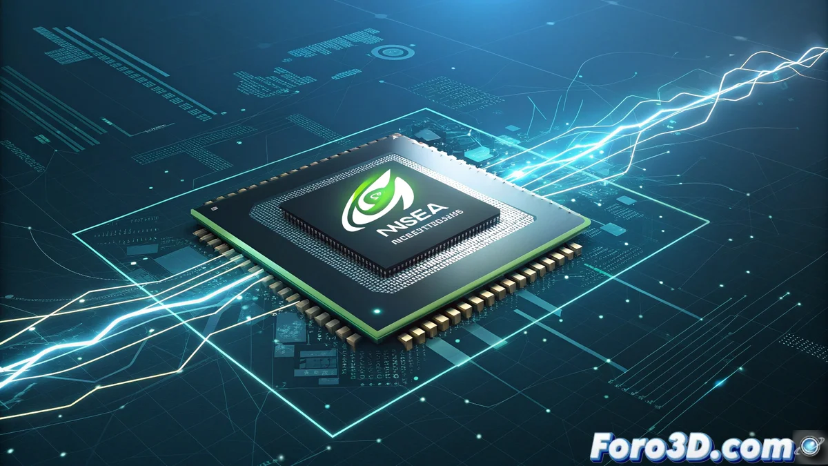
Technical Features of HBM3E Memory
Samsung's new HBM3E memory offers an impressive bandwidth of up to 1.2 TB/s per stack, significantly surpassing previous generations and providing the processing capacity needed for the most demanding requirements of modern artificial intelligence. This 12-layer technology stacks memory chips vertically, allowing for higher densities in a reduced space, ideal for AI accelerators where every square millimeter counts. Energy efficiency is also improved, a critical factor in large-scale data centers.
Implications for the Artificial Intelligence Ecosystem
Nvidia's certification positions Samsung as a qualified supplier alongside SK hynix and Micron, creating a triumvirate in the supply of high-end memory for the industry. This development is particularly significant considering the growing demand for AI solutions and the shortages that have characterized the semiconductor market in recent years.
- Increased competition: Three main suppliers instead of two.
- Price stabilization: Greater supply to meet growing demand.
- Accelerated innovation: Competition driving technical improvements.
- Supply security: Reduction in dependence on a single manufacturer.
Nvidia's certification validates not only Samsung's current product but also its ability to remain at the technological forefront.
Immediate Impact and Future Projections
Although deliveries to Nvidia will not begin until 2026, the announcement has had an immediate effect on Samsung's market valuation. Investors recognize the long-term potential of this partnership, especially considering that the AI accelerator market continues to expand at an exponential rate. Samsung's mass production capacity could become a determining factor in meeting global demand for artificial intelligence solutions.
Competitive Advantages of HBM3E Technology
The 12-layer architecture enables unprecedented density in memory packaging, essential for AI applications that require processing enormous volumes of data simultaneously. The 1.2 TB/s bandwidth facilitates the continuous feeding of information to graphics processing units, eliminating bottlenecks that could slow down the training of complex models. 🔥
The Competitive Landscape is Redefined
With this certification, Samsung positions itself in a strategic position for growth in the most profitable segment of semiconductors. The company has demonstrated its ability to match and possibly surpass its direct competitors in cutting-edge technology. The timing is particularly favorable, coinciding with the explosion of generative AI applications that demand ever-increasing amounts of high-performance memory.
Preparing for Large-Scale Production
The period until 2026 will allow Samsung to optimize its manufacturing processes to ensure production volumes that meet the anticipated demand from Nvidia and other potential customers. Scalability will be a key factor, considering that major AI accelerator manufacturers plan to significantly increase their production in the coming years.
With this certification, Samsung can feel so confident that even the most basic smartwatch in its production line could boast of having cousins working in AI servers. The semiconductor family has never been so united. 😄