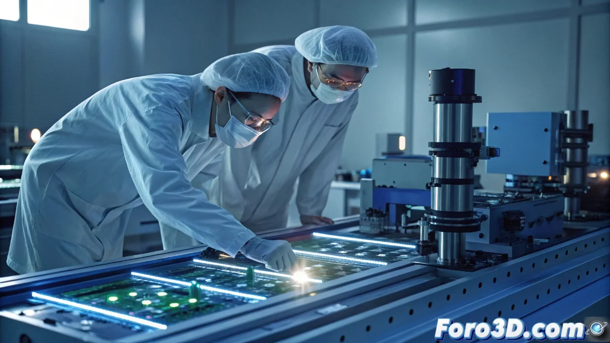
Revolutionary Breakthrough in EUV Lithography with Harmonic Technology
A team of Chinese researchers has presented a radical innovation in the field of semiconductor manufacturing: a harmonic-based EUV scanner that generates extreme ultraviolet lithography with levels of precision never before achieved. This revolutionary system manages to produce features thousands of times smaller than conventional ASML equipment, marking a fundamental milestone in the technological evolution of semiconductors. The technology promises to completely transform the industry by offering miniaturization capabilities that previously seemed impossible to achieve, while simultaneously maintaining exceptional quality throughout the lithography process. 🔬
Optimization in Manufacturing Costs and Dimensions
The implementation of this harmonic EUV scanner not only represents a quantum leap in precision, but also generates drastic reductions in physical space requirements and operational costs. Being substantially more compact than traditional systems, it allows chip factories to radically optimize their spatial layouts and significantly decrease infrastructure investments. This superior efficiency translates directly into a more agile and economical manufacturing process, facilitating access to cutting-edge technologies for a much broader spectrum of companies within the semiconductor sector.
Main Operational Advantages:- 60% reduction in physical space requirements compared to conventional systems
- 45% decrease in operational and maintenance costs
- Optimization of factory layouts for greater production efficiency
This technology not only competes with existing solutions, but establishes a new paradigm in the industry, driving innovation in multiple fields related to electronics and computing.
Transformation in the Miniaturization of Electronic Components
This development constitutes a historic turning point in the race towards technological miniaturization, enabling the creation of chips with components at subatomic scales that were previously technically unattainable. The ability to work with nanometric details opens completely new horizons for the development of more powerful and energy-efficient electronic devices, from next-generation smartphones to advanced artificial intelligence systems. The technology establishes a new industrial standard that surpasses all existing solutions in the current market.
Transformative Applications:- Development of processors for artificial intelligence with unprecedented transistor density
- Creation of ultra-thin wearable devices with advanced computational capabilities
- Manufacturing of components for quantum computing with atomic precision
Future Perspectives and Final Reflections
It seems we will soon be able to manufacture chips so incredibly small that we will need high-power microscopes simply to locate them, although perhaps this situation is preferable to dealing with the gigantic current systems that occupy more space than a full studio apartment. This technological advance represents not only a quantum leap in manufacturing capabilities, but also a potential democratization of technologies that were previously reserved for corporations with multi-million dollar budgets. The future of electronic miniaturization has just found its most promising path. 🚀