Researchers Manufacture Infrared Photodetectors with 3D Printing
A group of scientists from King Abdullah University of Science and Technology has presented a new approach to producing infrared light sensors using additive manufacturing technology. This achievement enables creating these electronic components more efficiently and with fewer resources, expanding their potential in various technological fields. Photodetectors are essential for detecting infrared radiation, invisible to humans but with a wide spectrum of practical uses. 🔬
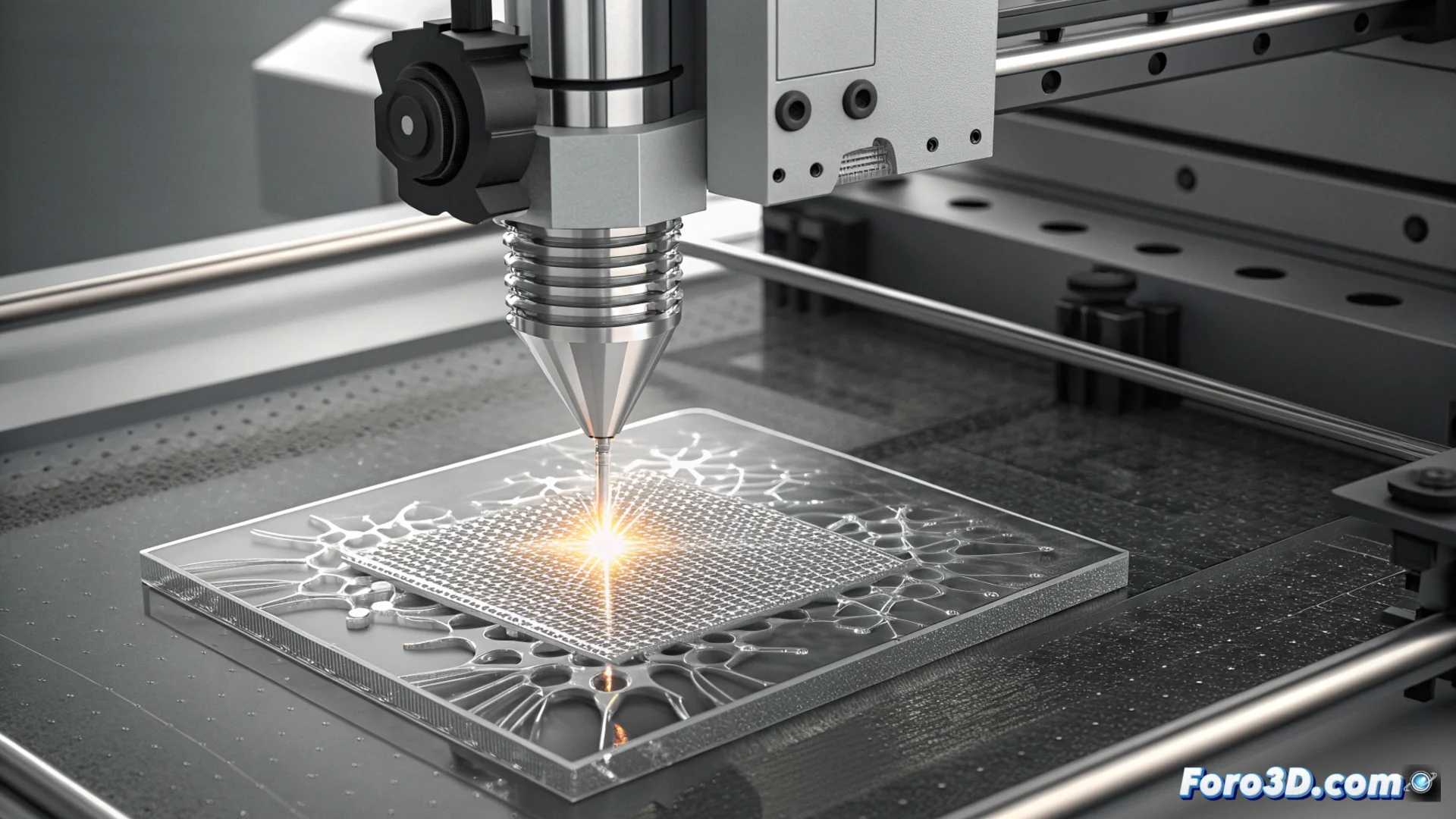
The Nanoparticle Injection Manufacturing Process
The technique is based on a 3D injection printer that precisely places silver nanoparticles on a bendable base material. This first layer forms the device's electrical contacts. Subsequently, a functional layer made of semiconductor nanocrystals is deposited. These tiny crystals react when exposed to infrared light, generating an electric current that serves to detect the radiation.
Key Features of the Method:- Uses a 3D printer that operates by injection to deposit materials.
- Utilizes silver nanoparticles to form conductive electrodes.
- The light-sensitive layer consists of specialized semiconductor nanocrystals.
3D printing transcends the realm of decorative objects to provide us with advanced sensory capabilities. Why use a special visor if you can integrate an infrared sensor directly into an accessory?
Practical Uses in Advanced Technology
These 3D-printed detectors can be incorporated into low-light vision equipment, allowing observation in the dark. They are also valuable for medical instrumentation and in systems that transmit data via optical fibers. The ability to print them on flexible surfaces indicates future use in wearable technology or components with non-planar shapes, where conventional sensors have limitations.
Immediate Application Areas:- Night vision systems for security or navigation.
- Monitoring and diagnostic devices in the healthcare sector.
- Receivers for communications using optical fiber.
The Future of Printed Electronics
This advance highlights how 3D printing is transforming the manufacturing of specialized electronic components. By reducing costs and production times, it democratizes access to technologies that were previously complex and expensive to produce. The combination of nanostructured materials with flexible substrates opens the way to a new generation of smart, integrated, and adaptable devices. The boundary between creating an object and creating a functional sensor is blurring more and more. 🚀