Photonic Computing Advances from the Lab to Functional Prototypes
The technology that uses photons instead of electrons to process information is leaving experimental environments to materialize in more practical prototypes. Various companies and research institutes are developing chips that combine optical components with standard silicon architectures, enabling data handling at speeds close to that of light. This method is especially promising for performing artificial intelligence operations and handling communications with much lower energy consumption than conventional semiconductors, since it does not rely on the flow of electrons through resistances, generating much less heat. 🚀
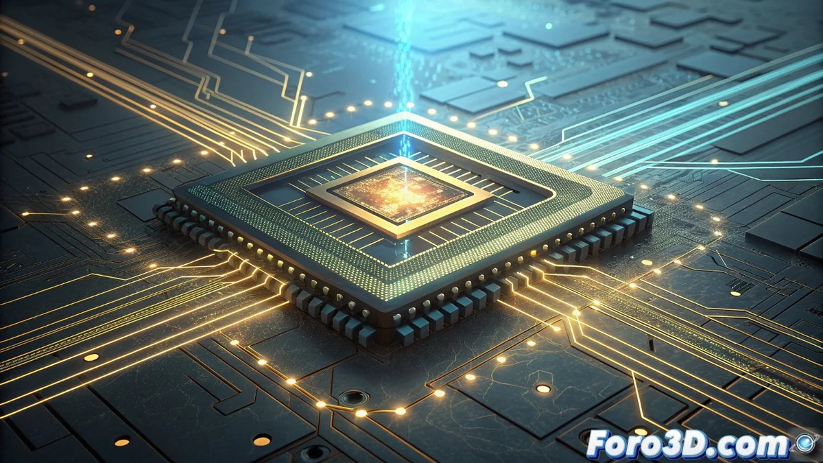
How Are Data Transported with Light on a Chip?
In a photonic integrated circuit, microscopic-scale lasers produce light pulses that travel through waveguides, tiny channels etched into the silicon substrate. These photons can be modulated to represent binary information, and elements like modulators, splitters, and optical detectors handle manipulating that signal. The key advantage is that light does not dissipate heat in the same intense way as an electric current. Additionally, multiple signals with different wavelengths can coexist in the same channel without interfering, inherently increasing bandwidth.
Key Components of a Photonic Chip:- Microscopic Lasers: Generate the light that carries the information.
- Waveguides: Channels that direct and confine light beams through the chip.
- Optical Modulators: Alter the properties of light to encode data.
- Photonic Detectors: Convert light signals back into electrical signals for interpretation.
Light does not generate the same thermal dissipation as an electric current, and multiple signals can travel through the same channel without interfering.
The Technical Challenges Still Hindering Mass Adoption
Although the scientific foundation is robust, manufacturing these systems at scale presents considerable difficulties. Miniaturizing and aligning components like lasers, filters, and detectors with nanometric precision on a single silicon chip is complex and costly. Another major obstacle is that current technology still needs to convert electrical signals to optical and vice versa at multiple points in the system, introducing latency and consuming additional energy. For these reasons, the first optical processors are unlikely to replace general-purpose CPUs, but rather act as specialized accelerators within hybrid configurations, handling highly parallel computations where their advantage in speed and efficiency is decisive.
Main Current Challenges:- Manufacturing and Alignment: Miniaturization and precise positioning of optical components at the nanoscale.
- Signal Conversion: The current need to translate between electrical and optical domains, adding complexity.
- Robustness and Stability: Systems must be stable enough to operate outside controlled lab environments.
The Future: Fully Optical Computers?
The vision of a fully optical computer that makes copper wires and traditional electronic circuits obsolete remains a long-term goal. For now, the industry's focus is on perfecting these chips to make them practical and robust, capable of functioning in real-world environments without external factors compromising their delicate internal optics. Progress is steady, and each new prototype brings photonic computing closer to specific commercial applications where its potential can be fully exploited. 🔦