ASML's Extreme Ultraviolet Lithography Machine: Manufacturing Chips at the Nanometer Scale
The technology for producing semiconductors takes a leap forward with extreme ultraviolet (EUV) lithography. These systems, designed by ASML, are essential for creating the densest and most powerful integrated circuits currently available. 🚀
Generating Light at a Minuscule Scale
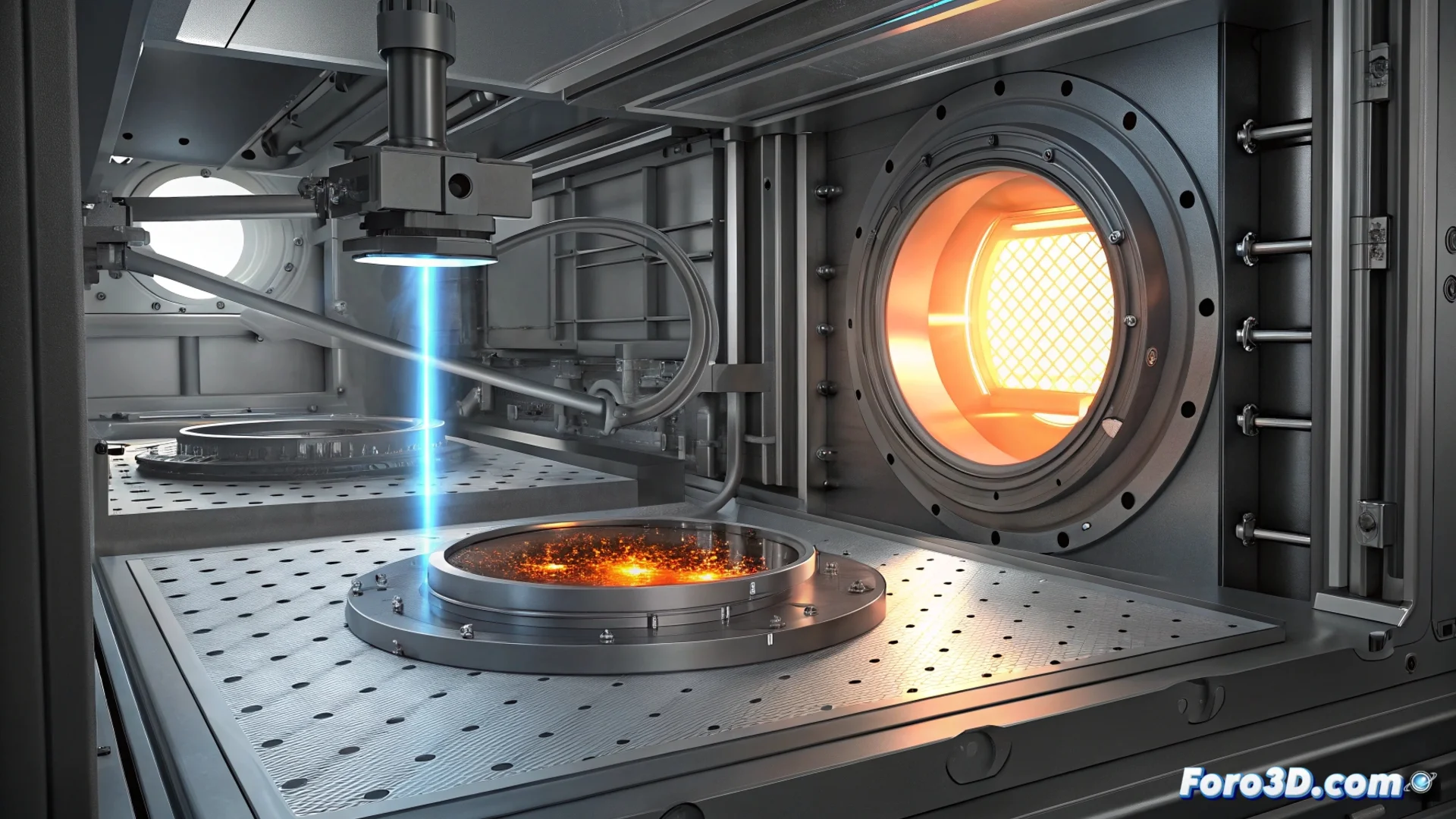
The core process of this machine relies on using light with a wavelength of just 13.5 nanometers. To produce this EUV light, the system transforms droplets of molten tin into a brilliant plasma. This light is the only one capable of etching incredibly small circuit patterns onto silicon wafers.
The Heart of the EUV System:- A powerful CO2 laser strikes falling tin droplets inside a vacuum chamber.
- The instantaneous impact converts the tin into plasma, which emits the crucial extreme ultraviolet light.
- A set of special mirrors, made with alternating layers of molybdenum and silicon, capture and direct this light with extreme precision.
These mirrors are among the flattest ever manufactured; the slightest imperfection would ruin the entire chip pattern.
Precision That Redefines Limits
The machine, known as the EXE:5200 model, aligns and exposes the wafer layer by layer. Its capability defines the scale of transistors, achieving critical dimensions below 10 nanometers. This enables the integration of tens of billions of transistors into a single chip.
Critical Operating Conditions:- The entire process must occur in an almost perfect vacuum, as air would absorb the EUV light.
- The wafer moves and adjusts with accuracy comparable to sinking a golf ball from continental distance.
- This transistor density is fundamental for powering artificial intelligence and high-performance computing.
A Pillar for Future Electronics
Without EUV lithography technology, further advances in electronic circuit miniaturization would be practically impossible. This equipment not only manufactures today's chips but also lays the foundation for the next generation of electronic devices. Its delicate operation and nanometer precision make it one of the most complex machines ever built. ⚙️