Extreme Ultraviolet Lithography: Revolution in Semiconductor Manufacturing
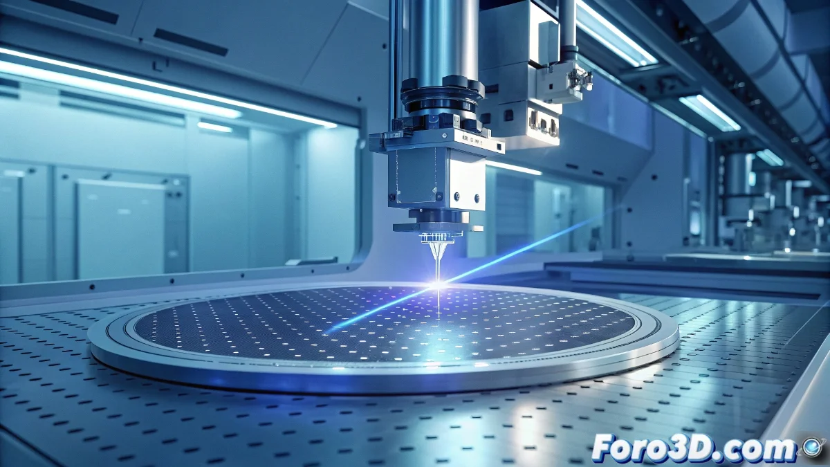
Extreme Ultraviolet Lithography (EUV) represents a fundamental technological advancement in the production of integrated circuits, using radiation with wavelengths of just 13.5 nanometers. This innovative method enables the etching of nanoscopic structures on silicon wafers, being crucial for developing transistors at 3 nm and 5 nm scales. The achieved precision allows integrating millions of components in reduced areas, optimizing the performance and energy efficiency of contemporary processors 🚀
Strategic Benefits of EUV Technology
The implementation of EUV systems transforms manufacturing processes by significantly reducing the number of stages required to build the complex layers of a chip. Unlike conventional techniques that needed multiple patterning, EUV achieves superior resolutions with fewer masks and alignment adjustments. This simplification not only speeds up manufacturing but also reduces imperfections, generating more efficient chips with lower energy demand, perfect for smartphones and high-end servers.
Key Advantages of EUV Lithography:- Reduction of up to 40% in manufacturing steps compared to previous methods
- Greater precision in patterns with tolerances below 1 nanometer
- Minimization of structural defects and improvement in final performance
EUV has overcome physical barriers that seemed insurmountable, allowing the continuation of the integration scaling predicted by Moore's Law
Transformation of the Semiconductor Landscape
The widespread adoption of EUV lithography marks a turning point in the miniaturization of electronic components. Tech giants like TSMC and Samsung have integrated this methodology to remain competitive, developing processors that power innovations in artificial intelligence, cloud computing, and mobile devices. With the continuous reduction of nodes, EUV consolidates as a technological pillar to overcome physical limitations, ensuring that semiconductor evolution continues for the next decade.
Notable Industrial Impacts:- Acceleration in the development of chips for AI and machine learning applications
- Reduction of operational costs in manufacturing plants in the long term
- Ability to produce components with unprecedented densities
Future and Prospects of Miniaturization
Transistors have reached such tiny dimensions that engineers joke about needing protection from their own concentrated power. EUV technology continues to evolve to face new challenges in semiconductor manufacturing, promising even more surprising advances in the coming years. This technological revolution ensures that we can continue enjoying more powerful and efficient devices, demonstrating that innovation in nanofabrication is far from reaching its limits 🎯