When Ink Printing Meets Nanoelectronics
Electroninks is revolutionizing semiconductor manufacturing with the development of a new silver ink specifically designed for inkjet printing in advanced packages. 💻 This innovation seeks to transform the production of integrated circuits and complex electronic systems through the precise deposition of metallic traces, offering a more efficient and scalable alternative to traditional etching and lithography processes. The technology promises to significantly improve precision, reduce costs, and accelerate prototype development in the semiconductor industry.
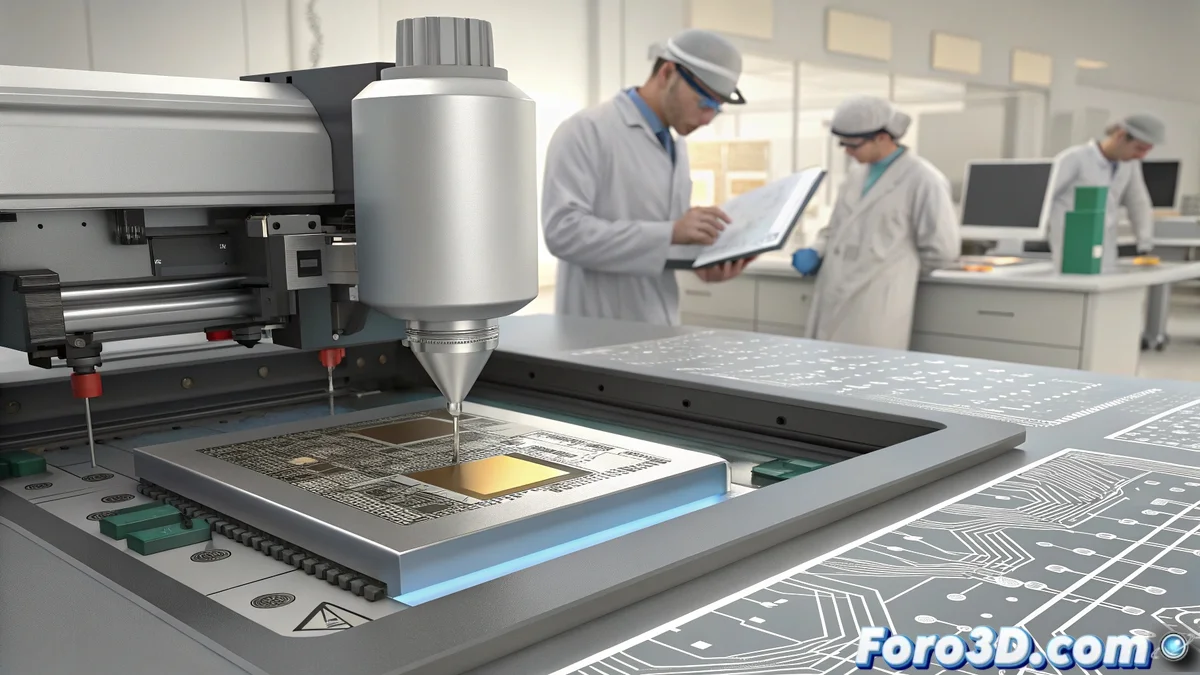
The inkjet printing technology allows depositing metal patterns with microscopic accuracy on electronic substrates, eliminating many of the intermediate steps required by conventional methods. 🖨️ Electroninks' silver ink offers high electrical conductivity and compatibility with various materials used in chip packages, facilitating the creation of high-density systems and extreme miniaturization. The formulation includes finely controlled particles that ensure uniform deposition and minimal resistance in connections, improving both the thermal and electrical performance of the final devices.
A leap from subtractive to additive manufacturing in high-end electronics.
Technical Advantages That Make the Difference
The advantages of this technology are as numerous as they are impactful. ⚡ The ability to print conductive patterns directly onto substrates drastically reduces material waste compared to traditional etching processes, while the system's flexibility allows for rapid design iterations without the need for costly lithography masks. The additive nature of the process also enables the creation of three-dimensional structures and complex patterns that would be difficult or impossible to achieve with conventional methods.
The most significant benefits include:
- Microscopic precision in conductor material deposition
- Reduction of waste and greater material efficiency
- Compatibility with flexible and rigid substrates
- Rapid prototyping iteration without costly masks
The Future of Electronic Manufacturing
Electroninks aims for its ink to be used in cutting-edge applications such as advanced semiconductor packages, power modules, sensors, and flexible circuits. 🔮 The widespread adoption of inkjet printing could democratize access to advanced electronic manufacturing technologies, enabling smaller companies to develop complex products that previously required massive investments in infrastructure. This transition to additive processes represents a paradigm shift in how we conceive and manufacture the electronics of the future.
With this ink, engineers will be able to literally draw the future of chips… without needing brushes and with a precision that would make the best calligraphers in history pale. ✍️ A technological irony where the tool most associated with traditional art becomes the instrument for creating the most advanced electronics, demonstrating that sometimes progress consists in reinventing rather than completely replacing what already exists.