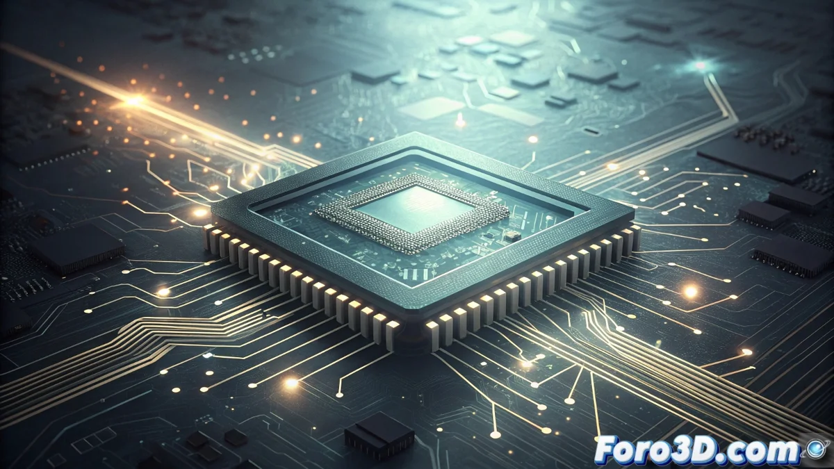
Backside Power Delivery: An Advance in Semiconductors
Imagine a world where electronic chips operate with greater fluidity and efficiency, as if we had taken a giant step toward the future of technology. This technique, known as backside power delivery, revolutionizes the semiconductor industry by relocating the power lines to the back of the silicon, thus isolating the power paths from the data paths on the main surface. The result is a notable reduction in electromagnetic interference and a denser interconnection, which elevates the overall performance of processors to impressive levels. 😎
Innovative Advantages of This Technology
In my opinion, as an expert on these topics, this innovation is not limited to improving power flow; it also transforms the way we design electronic devices. By eliminating conflicts between data signals and power, manufacturers gain valuable space on the chip, which translates into faster processors and superior thermal management. This is especially vital for high-computing applications, where every detail counts to avoid overheating and maximize energy efficiency.
Key Advantages:- Minimizes energy consumption by optimizing paths, allowing devices that last longer with the same battery, ideal for everyday gadgets.
- Facilitates more compact designs, opening doors to thinner and more portable electronic products without sacrificing power.
- Improves thermal efficiency, crucial for avoiding failures in high-performance environments, such as servers or gaming equipment.
This technology, although it seems taken from a futuristic story, reminds us that true advancement lies in practicality: "In the end, they still need a plug to shine," as a touch of reality amid innovation.
Transformative Impact on the Future
From my perspective, backside power delivery is not just a step forward; it is a leap that drives the creation of more powerful and eco-friendly chips. This separation of components allows scaling transistor density without risks, fostering advances in artificial intelligence and mobile devices. We are talking about hardware that surpasses current barriers, such as chips that process data at dizzying speeds while maintaining sustainability. 🚀
Key Aspects of the Impact:- Boosts developments in artificial intelligence, enabling more complex algorithms in everyday devices without increasing consumption.
- Opens opportunities in mobile devices, with batteries that last longer and stable performance for demanding apps.
- Facilitates transistor scalability, overcoming limitations to generate future generations of innovative and efficient hardware.
Final Conclusion and Reflections
In summary, backside power delivery marks a milestone in the evolution of semiconductors, offering not only immediate improvements in efficiency and performance, but also a path toward more sustainable technologies. As a passionate writer about these advances, I believe this innovation brings us closer to a world where devices are smarter and more eco-friendly, while always keeping our feet on the ground. Remember, it's not magic, but brilliant engineering that redefines what is possible. 🌟