ASML Launches the Revolutionary Twinscan XT:360 Lithography Scanner for 3D Chip Packaging
ASML, the global leader in semiconductor lithography systems, has announced the launch of the revolutionary Twinscan XT:360 scanner, specifically designed for advanced 3D chip packaging. This new machine represents a transformative breakthrough in semiconductor manufacturing, achieving quadruple the throughput compared to previous systems and setting a new industry standard. 💡
A Quantum Leap in 3D Packaging
The Twinscan XT:360 is specifically optimized for the demanding requirements of advanced 3D packaging, a crucial technology for the future of semiconductors. By quadrupling throughput, ASML enables chipmakers to produce more complex devices more efficiently, addressing one of the most significant bottlenecks in modern semiconductor manufacturing. 🔬
Key Features of the Twinscan XT:360:- Quadruple the throughput compared to previous generations
- Specifically optimized for advanced 3D packaging
- Greater precision in aligning multiple chip layers
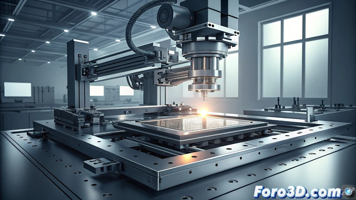
The Twinscan XT:360 quadruples throughput, setting a new record in production efficiency
Lithography Technology for the Next Generation of Chips
The system incorporates significant technological advances in optics, precision, and processing speed. The ability to quadruple throughput not only improves production efficiency but also significantly reduces the cost per chip, making advanced 3D packaging technologies more accessible for a wider range of applications, from mobile devices to data centers. 📱
Technical Advances Implemented:- Ultra-high precision alignment systems
- Enhanced optics for higher resolutions
- Advanced automation of the production process
Impact on the Semiconductor Industry
This launch comes at a critical time for the semiconductor industry, where the demand for more powerful and efficient chips continues to grow exponentially. The Twinscan XT:360 will allow manufacturers to accelerate the development of 3D devices that combine multiple chips in a single package, an essential technology for AI applications, high-performance computing, and edge devices. 🚀
Key Applications Benefited:- Processors for artificial intelligence and machine learning
- Chips for data centers and cloud computing
- Next-generation mobile devices
The Future of Semiconductor Manufacturing
With the Twinscan XT:360, ASML consolidates its leadership in lithography technology and lays the groundwork for the next generation of semiconductor advances. This innovation not only addresses the current needs of the industry but also enables new architectural possibilities in chip design, driving innovation across multiple technology sectors and ensuring that Moore's Law continues to evolve through advanced 3D packaging. ✨