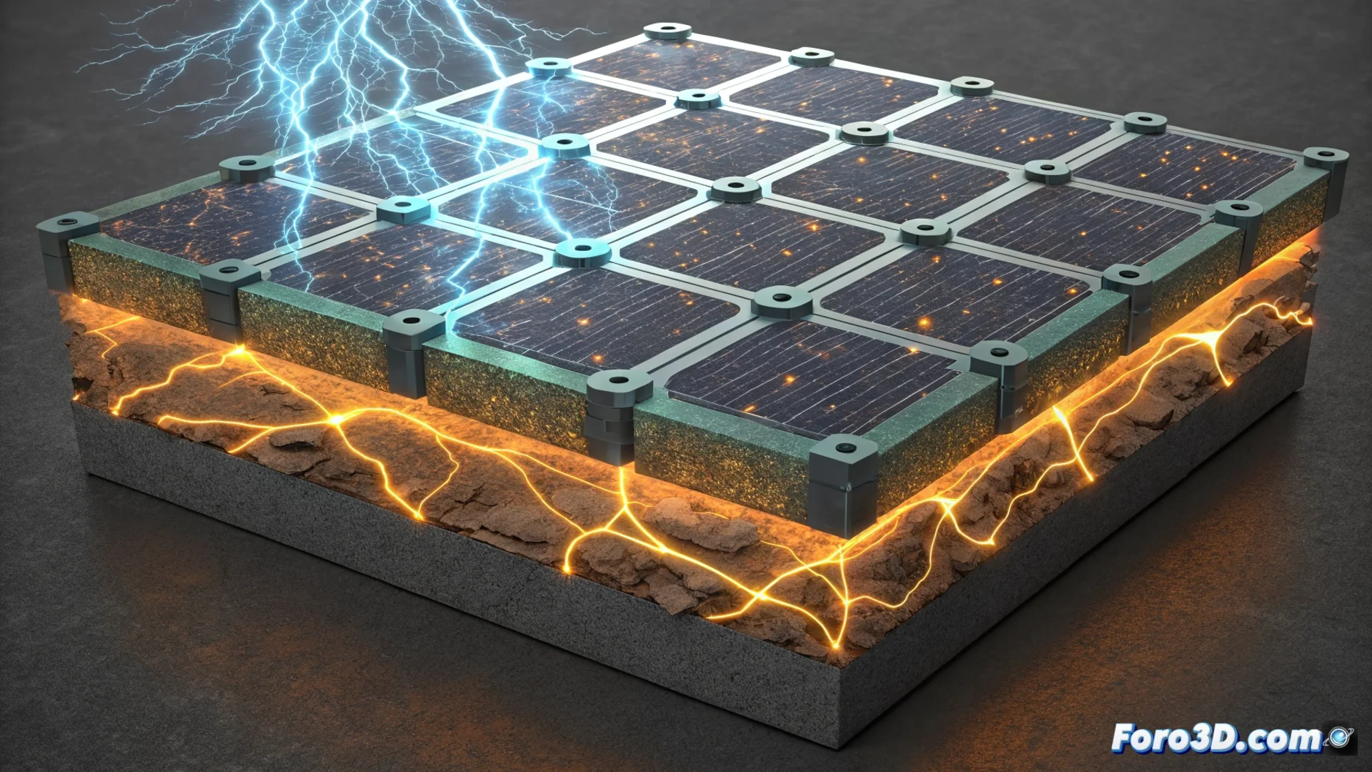
An electrical CT scan reveals how passivation improves perovskites
Science advances with a revolutionary diagnostic tool for solar energy. A group of scientists has adapted a non-invasive imaging technique, analogous to a medical CT scanner, to inspect the interior of perovskite solar cells. This method, dubbed electrical CT, allows observing with unprecedented precision how electrons move within the semiconductor material. 🔬
Diagnosing cracks in electron flow
The power of this technique lies in its ability to directly map the path of electrical current. The obtained images leave no doubt: they reveal specific areas where the current slows down, gets blocked, or diverted. These electrical bottlenecks are the main cause limiting the final efficiency of these promising photovoltaic devices. Visualizing the problem is the fundamental first step to solving it.
What the electrical CT allows discovering:- Blockage points: Identifies microscopic regions where charge carriers (electrons and holes) cannot circulate freely.
- Current deviations: Shows alternative routes that electricity takes when encountering obstacles, generating energy losses.
- Material heterogeneity: Evidences how the quality and uniformity of the perovskite crystal directly affect its conductivity.
This ability to see inside the material without damaging it represents a powerful tool for developing more stable and efficient perovskites.
Passivation as a restorative treatment
The research does not stop at diagnosis. The study applied this electrical CT to evaluate the effect of passivating agents. These chemical compounds are used to "heal" defects in the perovskite's crystal lattice. The comparative images are eloquent: after passivation, the current flows notably more uniformly and encounters many fewer obstacles in its path.
Microscopic effects of passivation:- Repair defects: Passivators seal cracks and voids in the atomic structure that trap charge carriers.
- Homogenize the flow: Electricity is distributed more equitably across the entire active area of the cell.
- Increase voltage: By reducing recombination losses, the open-circuit voltage is directly increased, a key performance parameter.
A future guided by internal vision
This technology shifts material development from a trial-and-error process to one guided by direct visual evidence. Engineers can now correlate specific treatments with their real impact on the device's electrical nanostructure. This allows optimizing coatings, chemical compositions, and manufacturing methods much faster and more targetedly. The ultimate goal is clear: use this internal vision to accelerate the arrival of more efficient and stable perovskite solar cells to the large-scale commercial market. ⚡