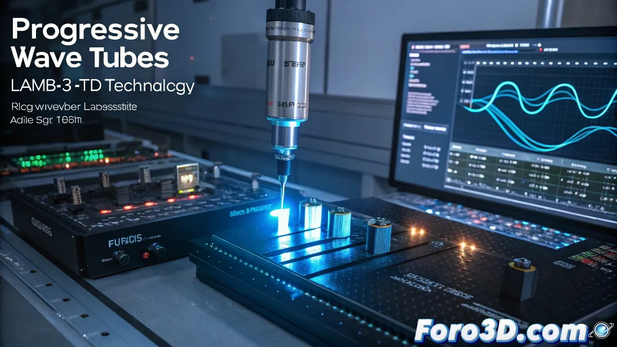
A Revolutionary Breakthrough in Traveling Wave Tube Manufacturing
The American startup Elve has developed a new manufacturing process that drastically reduces the production time for traveling wave tubes (TWTs), essential components in high-frequency applications such as satellite communications and radar systems. While it previously took over a year to manufacture these devices, the new method, called Layered Additive Multi-Material Manufacturing – Digitized (LAM3D), allows production to be completed in just a few weeks. This breakthrough has been made possible with support from the Defense Advanced Research Projects Agency (DARPA).
The Importance of Traveling Wave Tubes
TWTs are fundamental in applications such as satellite communications, deep space exploration, and electronic warfare systems. However, their traditional manufacturing has faced challenges due to the complexity of their designs and the need for extremely precise assemblies. The new LAM3D method not only simplifies this process but also significantly speeds it up, allowing for greater production efficiency.
Rapid Design and Advanced Optimization
One of the most notable advantages of the LAM3D process is its ability to design and optimize TWT circuits in less than two hours. This is possible for different frequency bands, such as Q-band (33–50 GHz), V-band (40–75 GHz), and E-band (60–90 GHz), which are fundamental for advanced radar systems and high-speed communication networks. This flexibility allows components to be adapted to a wide range of applications, from defense to the commercial sector.
"The LAM3D process not only improves efficiency but also democratizes access to high-frequency technologies."
Strategic Support and Funding
Elve has not only received technical support from DARPA but has also had the assistance of the agency's Entrepreneurship and Economic Development Initiative (EEI) to develop its market strategy. Furthermore, the startup has secured $15 million in a Series A funding round, which has allowed it to establish a commercial manufacturing facility. This financial and strategic backing has been key to taking the technology to the next level.
Expansion into Higher Frequencies
The LAM3D process has evolved to produce circuits operating above 200 GHz, opening up new possibilities for future communication and detection technologies. This advance not only benefits defense applications but also has a significant impact on the commercial sector, increasing the availability of TWTs for a variety of uses.
- Efficiency: Reduction of production time from over a year to just weeks.
- Precision: Circuit design and optimization in less than two hours.
- Versatility: Adaptation to different frequency bands, from Q-band to E-band.
In summary, Elve's innovation represents a significant step towards modernizing the manufacturing of critical components. By reducing production times and increasing precision, the LAM3D process not only improves efficiency but also democratizes access to high-frequency technologies. This breakthrough could transform entire industries, from communications to defense, offering faster and more accessible solutions for the technological challenges of the future.