A study simulates how hydrogen activates p-type gallium nitride
A group of researchers uses advanced computational modeling to decipher a vital step in producing gallium nitride (GaN) with magnesium, a p-type semiconductor material. These ab initio simulations recreate the path that hydrogen atoms follow within the crystal and how they manage to exit to the outside during a heat treatment. This element is fundamental because, during material growth, it deactivates the magnesium atoms that must capture holes to enable p-type conduction. For the semiconductor to operate, it is essential that this hydrogen be removed. 🔬
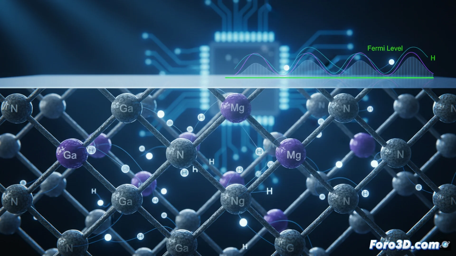
The exit gate is defined by the surface Fermi level
The work reveals that the element that decides everything is the location of the Fermi level on the outer face of the GaN. This energy parameter acts as a boundary that can block or facilitate hydrogen exit. When the Fermi level on the surface is in a low position, hydrogen faces a high barrier and remains trapped inside, leaving the material inactive. If, on the contrary, this level is high, hydrogen can move and detach much more easily. This knowledge enables establishing the ideal hydrogen partial pressure inside the annealing furnace: it must be low to allow evacuation, but not so low that it damages the semiconductor's surface integrity.
Key points of the activation mechanism:- Ab initio simulations model atomic dynamics with high precision.
- The surface Fermi level acts as an energy switch that controls migration.
- Optimizing hydrogen pressure during annealing is crucial to activate the material without degrading it.
Controlling precisely how hydrogen escapes is what allows transforming an inert crystal into a functional and efficient p-type semiconductor.
Why p-type GaN is vital in our technology
Mastering and perfecting this mechanism has enormous industrial importance. P-type GaN is an irreplaceable component in optoelectronic devices such as light-emitting diodes (LEDs), lasers, and displays, and it is also key in power electronics for fast adapters and systems that manage energy with higher performance. By being able to precisely control how the semiconductor is activated, devices can be manufactured that consume less electricity, last longer, and have a lower production cost, directly impacting everyday technology.
Direct applications of optimized p-type GaN:- Lighting and displays: Brighter and more efficient LEDs for screens and lighting.
- Power electronics: Smaller ultra-fast chargers with less energy loss.
- Energy management systems: Equipment that converts and distributes electricity with higher efficiency.
A small atom with a big impact
So, the next time your fast charger stops working, the problem might not be in the plug. It could be due to the fact that, during its manufacturing, a hydrogen atom refused to leave its comfortable spot within the GaN crystal lattice, preventing the p-type semiconductor from activating correctly. This study, through simulation, illuminates the path to avoid precisely that. 💡